
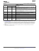
Datasheet
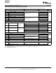

PWM
CONTROLLER
+12V
+100V
SECONDARY
SIDE
CIRCUIT
HI
CONTROL
DRIVE
LO
DRIVE
HI
V
DD
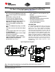
UCC27211
VSS
LI
HB
HO
HS
LO
+12V
HI
CONTROL
DRIVE
LO
DRIVE
HI
VDD
UCC27211
LI
HB
HO
HS
LO
+100V
PWM
CONTROLLER
+12V
ISOLATION
AND
FEEDBACK
+100V
SECONDARY
SIDE
CIRCUIT
HI
CONTROL
DRIVE
LO
DRIVE
HI
V
DD
UCC27210
VSS
LI
HB
HO
HS
LO
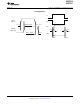
UCC27210
UCC27211
www.ti.com
SLUSAT7E –NOVEMBER 2011–REVISED AUGUST 2013
120-V Boot, 4-A Peak, High Frequency High-Side and Low-Side Driver
Check for Samples: UCC27210, UCC27211
1
FEATURES
APPLICATIONS
2
• Drives Two N-Channel MOSFETs in High-Side
• Power Supplies for Telecom, Datacom, and
and Low-Side Configuration with Independent Merchant
Inputs
• Half-Bridge and Full-Bridge Converters
• Maximum Boot Voltage 120-V DC
• Push-Pull Converters
• 4-A Sink, 4-A Source Output Currents
• High Voltage Synchronous-Buck Converters
• 0.9-Ω Pull-Up and Pull-Down Resistance
• Two-Switch Forward Converters
• Input Pins can Tolerate -10 V to 20 V and are
• Active-Clamp Forward Converters
Independent of Supply Voltage Range
• Class-D Audio Amplifiers
• TTL or Pseudo-CMOS Compatible Input
Versions
DESCRIPTION
• 8-V to 17-V VDD Operating Range, (20-V ABS
The UCC27210 and UCC27211 Drivers are based on
MAX)
the popular UCC27200 and UCC27201 MOSFET
drivers, but offer several significant performance
• 7.2-ns Rise and 5.5-ns Fall Time with 1000-pF
improvements. Peak output pull-up and pull-down
Load
current has been increased to 4-A source and 4-A
• Fast Propagation Delay Times (18 ns typical)
sink, and pull-up and pull-down resistance have been
• 2-ns Delay Matching
reduced to 0.9 Ω, thereby allowing for driving large
power MOSFETs with minimized switching losses
• Symmetrical Under Voltage Lockout for High-
during the transition through the MOSFET’s Miller
Side and Low-Side Driver
Plateau. The input structure is now able to directly
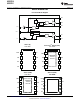
• All Industry Standard Packages Available
handle -10 VDC, which increases robustness and
(SOIC-8, PowerPAD™ SOIC-8, 4-mm x 4-mm
also allows direct interface to gate-drive transformers
SON-8 and 4-mm x 4-mm SON-10)
without using rectification diodes. The inputs are also
independent of supply voltage and have a 20-V
• Specified from -40 to 140 °C
maximum rating.
Typical Application Diagrams
1
Please be aware that an important notice concerning availability, standard warranty, and use in critical applications of
Texas Instruments semiconductor products and disclaimers thereto appears at the end of this data sheet.
2PowerPAD is a trademark of Texas Instruments.
PRODUCTION DATA information is current as of publication date.
Copyright © 2011–2013, Texas Instruments Incorporated
Products conform to specifications per the terms of the Texas
Instruments standard warranty. Production processing does not
necessarily include testing of all parameters.