
Datasheet

SLUS486B − AUGUST 2001 − REVISED JULY 2003
1
www.ti.com
FEATURES
Maximizes Efficiency by Minimizing
Body-Diode Conduction and Reverse
Recovery Losses
Transparent Synchronous Buck Gate Drive
Operation From the Single Ended PWM Input
Signal
12-V or 5-V Input Operation
3.3-V Input Operation With Availability of
12-V Bus Bias
On-Board 6.5-V Gate Drive Regulator
±3.3-A TrueDrive Gate Drives for High
Current Delivery at MOSFET Miller
Thresholds
Automatically Adjusts for Changing
Operating Conditions
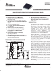
Thermally Enhanced 14-Pin PowerPAD
HTSSOP Package Minimizes Board Area and
Junction Temperature Rise
APPLICATIONS
Non-Isolated Single or Multi-phased
DC-to-DC Converters for Processor Power,
General Computer, Telecom and Datacom
Applications
DESCRIPTION
The UCC27221 and UCC27222 are high-speed
synchronous buck drivers for today’s
high-efficiency, lower-output voltage designs.
Using Predictive Gate Drive (PGD) control
technology, these drivers reduce diode
conduction and reverse recovery losses in the
synchronous rectifier MOSFET(s). The
UCC27221 has an inverted PWM input while the
UCC27222 has a non-inverting PWM input.
Predictive Gate Drive technology uses control
loops which are stabilized internally and are
therefore transparent to the user. These loops use
no external components, so no additional design
is needed to take advantage of the higher
efficiency of these drivers.
This closed loop feedback system detects
body-diode conduction, and adjusts deadtime
delays to minimize the conduction time interval.
This virtually eliminates body-diode conduction
while adjusting for temperature, load- dependent
delays, and for different MOSFETs. Precise gate
timing at the nanosecond level reduces the
reverse recovery time of the synchronous rectifier
MOSFET body-diode, reducing reverse recovery
losses seen in the main (high-side) MOSFET. The
lower junction temperature in the low-side
MOSFET increases product reliability. Since the
power dissipation is minimized, a higher switching
frequency can also be used, allowing for smaller
component sizes.
The UCC27221 and UCC27222 are offered in the
thermally enhanced 14-pin PowerPAD package
with 2°C/W θ
jc
.
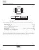
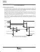
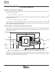
7
6,8
3
4,5
IN
GND
VDD
VLO
14
13
11,12
9,10
VHI
G1
SW
G2
UCC27222
PWM
IN
V
IN
GND
OU
T
V
OU
T
GND
IN
FUNCTIONAL APPLICATION DIAGRAM
Note: 12-V input system shown. For 5-V input only systems, see Figure 6.
! "#$ ! %#&'" ($)
(#"! " !%$""! %$ *$ $! $+! !#$!
!(( ,-) (#" %"$!!. ($! $"$!!'- "'#($
$!. '' %$$!)
Copyright 2002, Texas Instruments Incorporated
Predictive Gate Drive and PowerPAD are trademarks of Texas Instruments Incorporated.