
Datasheet
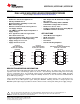
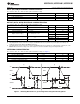
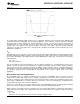

VDD
OUTA
NC
OUTB
INA
NC
GND
INB
1
2
3
4
8
7
6
5
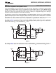
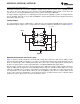
NC – No internal connection
UCC27323
(DUAL INVERTING)
D, DGN, OR P PACKAGE
(TOP VIEW)
VDD
OUTA
NC
OUTB
INA
NC
GND
INB
1
2
3
4
8
7
6
5
UCC27324
(DUAL NONINVERTING)
D, DGN, OR P PACKAGE
(TOP VIEW)
VDD
OUTA
NC
OUTB
INA
NC
GND
INB
1
2
3
4
8
7
6
5
UCC27325
(ONE INVERTING, ONE )
D, DGN, OR P PACKAGE
(TOP VIEW)
NONINVERTING
UCC27323-Q1, UCC27324-Q1, UCC27325-Q1
www.ti.com
SLUS678A –MARCH 2008–REVISED APRIL 2012
DUAL 4-A PEAK HIGH-SPEED LOW-SIDE POWER MOSFET DRIVERS
Check for Samples: UCC27323-Q1, UCC27324-Q1, UCC27325-Q1
1
FEATURES
2
• Qualified for Automotive Applications
• Dual Outputs Can Be Paralleled for Higher
Drive Current
• Industry-Standard Pinout
• Available in Thermally Enhanced MSOP
• High Current Drive Capability of ±4 A at the
PowerPAD™ Package with 4.7°C/W θ
JC
Miller Plateau Region
• Rated From –40°C to 125°C
• Efficient Constant Current Sourcing Even at
Low Supply Voltages • TrueDrive™ Output Architecture Using Bipolar
and CMOS Transistors in Parallel
• TTL-/CMOS-Compatible Inputs Independent of
Supply Voltage
APPLICATIONS
• 20-ns Typical Rise and 15-ns Typical Fall
• Switch-Mode Power Supplies
Times with 1.8-nF Load
• DC/DC Converters
• Typical Propagation Delay Times of 25 ns With
Input Falling and 35 ns With Input Rising
• Motor Controllers
• Supply Voltage of 4 V to 15 V
• Line Drivers
• Supply Current of 0.3 mA
• Class D Switching Amplifiers
DESCRIPTION/ORDERING INFORMATION
The UCC27323/UCC27324/UCC27325 high-speed dual MOSFET drivers can deliver large peak currents into
capacitive loads. Three standard logic options are offered — dual inverting, dual noninverting, and one inverting
and one noninverting driver. The thermally enhanced 8-pin PowerPAD™ MSOP package (DGN) drastically
lowers the thermal resistance to improve long-term reliability. The drivers are also offered in the standard SOIC-8
(D) or PDIP-8 (P) packages.
Using a design that inherently minimizes shoot-through current, these drivers deliver 4 A of current where it is
needed most, at the Miller plateau region during the MOSFET switching transition. A unique bipolar and
MOSFET hybrid output stage in parallel also allows efficient current sourcing and sinking at low supply voltages.
1
Please be aware that an important notice concerning availability, standard warranty, and use in critical applications of
Texas Instruments semiconductor products and disclaimers thereto appears at the end of this data sheet.
2PowerPAD, TrueDrive are trademarks of Texas Instruments.
UNLESS OTHERWISE NOTED this document contains
Copyright © 2008–2012, Texas Instruments Incorporated
PRODUCTION DATA information current as of publication date.
Products conform to specifications per the terms of Texas
Instruments standard warranty. Production processing does not
necessarily include testing of all parameters.