
Datasheet
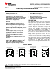
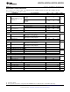
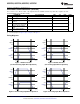
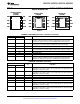
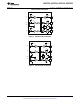
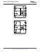
Table Of Contents
- FEATURES
- APPLICATIONS
- DESCRIPTION
- PRODUCT MATRIX
- DESCRIPTION (CONTINUED)
- ABSOLUTE MAXIMUM RATINGS
- RECOMMENDED OPERATING CONDITIONS
- THERMAL INFORMATION
- THERMAL INFORMATION
- ELECTRICAL CHARACTERISTICS
- DEVICE INFORMATION
- TYPICAL CHARACTERISTICS
- APPLICATION INFORMATION
- Introduction
- VDD and Under Voltage Lockout
- Operating Supply Current
- Input Stage
- Enable Function
- Output Stagean updated Output Stage section.
- Low Propagation Delays and Tightly Matched Outputs
- Drive Current and Power Dissipationupdated Drive Current and Power Dissipation section.
- Thermal Information
- PCB Layout
- REVISION HISTORY
1
2
3
4
ENA
INA
GND
INB
8
7
6
5
ENB
OUTA
VDD
OUTB
UCC27523
Dual Inverting Inputs
1
2
3
4
ENA
INA
GND
INB
8
7
6
5
ENB
OUTA
VDD
OUTB
UCC27524
Dual Non-Inverting Inputs
1
2
3
4
ENA
INA
GND
INB
8
7
6
5
ENB
OUTA
VDD
OUTB
UCC27525
One Inverting and One
Non-Inverting Input
1
2
3
4
INA-
INB-
GND
OUTB
8
7
6
5
INA+
INB+
OUTA
VDD
UCC27526
Dual Input Configuration
+
+
UCC27523, UCC27524, UCC27525, UCC27526
www.ti.com
SLUSAQ3F –NOVEMBER 2011–REVISED MAY 2013
Dual 5-A High-Speed Low-Side Gate Driver
Check for Samples: UCC27523, UCC27524, UCC27525, UCC27526
1
FEATURES
APPLICATIONS
2
• Industry-Standard Pin Out
• Switch-Mode Power Supplies
• Two Independent Gate-Drive Channels • DC-to-DC Converters
• 5-A Peak Source and Sink-Drive Current • Motor Control, Solar Power
• Independent-Enable Function for Each Output • Gate Drive for Emerging Wide Band-Gap
Power Devices such as GaN
• TTL and CMOS Compatible Logic Threshold
Independent of Supply Voltage
DESCRIPTION
• Hysteretic-Logic Thresholds for High Noise
The UCC2752x family of devices are dual-channel
Immunity
high-speed low-side gate-driver devices capable of
• Inputs and Enable Pin-Voltage Levels Not
effectively driving MOSFET and IGBT power
Restricted by VDD Pin Bias Supply Voltage
switches. Using a design that inherently minimizes
shoot-through current, UCC2752x is capable of
• 4.5 to 18-V Single-Supply Range
delivering high-peak current pulses of up to 5-A
• Outputs Held Low During VDD-UVLO, (ensures
source and 5-A sink into capacitive loads along with
glitch-free operation at power-up and power-
rail-to-rail drive capability and extremely small
down)
propagation delay typically 13 ns. In addition, the
• Fast Propagation Delays (13-ns typical)
drivers feature matched internal propagation delays
between the two channels which are very well suited
• Fast Rise and Fall Times (7-ns and 6-ns
for applications requiring dual-gate drives with critical
typical)
timing, such as synchronous rectifiers. This also
• 1-ns Typical Delay Matching Between 2-
enables connecting two channels in parallel to
Channels
effectively increase current-drive capability or driving
• Two Outputs are Paralleled for Higher Drive
two switches in parallel with a single input signal. The
input pin thresholds are based on TTL and CMOS
Current
compatible low-voltage logic, which is fixed and
• Outputs Held in LOW When Inputs Floating
independent of the VDD supply voltage. Wide
• PDIP-8, SOIC-8, MSOP-8 PowerPAD™ and 3-
hysteresis between the high and low thresholds offers
mm × 3-mm WSON-8 Package Options
excellent noise immunity.
• Operating Temperature Range of –40°C to
+140°C
PRODUCT MATRIX
1
Please be aware that an important notice concerning availability, standard warranty, and use in critical applications of
Texas Instruments semiconductor products and disclaimers thereto appears at the end of this data sheet.
2PowerPAD is a trademark of Texas Instruments.
PRODUCTION DATA information is current as of publication date.
Copyright © 2011–2013, Texas Instruments Incorporated
Products conform to specifications per the terms of the Texas
Instruments standard warranty. Production processing does not
necessarily include testing of all parameters.