
Datasheet
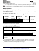
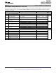

1
2
3
6
5
4
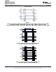
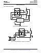
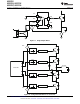
IN
EN
GND
OUTL
OUTH 1
2
3
5
4IN+
VDD
IN-
OUT 1
2
3
5
4
GND
IN-
EN 1
2
3
5
4IN+
EN 1
2
3
6
5
4
IN1
OUTL
IN2
OUTH
GND
GND
GND
VDD VDD
VDD
VDD
OUT OUT
UCC27531 UCC27533 UCC27536 UCC27537 UCC27538
UCC27531
UCC27533, UCC27536
UCC27537, UCC27538
www.ti.com
SLUSBA7D – DECEMBER 2012–REVISED APRIL 2013
2.5-A and 5-A, 35-V
MAX
VDD FET and IGBT Single-Gate Driver
Check for Samples: UCC27531 , UCC27533, UCC27536 , UCC27537, UCC27538
1
FEATURES
APPLICATIONS
• Low Cost Gate Driver (offering optimal • Switch-Mode Power Supplies
solution for driving FET and IGBTs)
• DC-to-DC Converters
• Superior Replacement to Discrete Transistor
• Solar Inverters, Motor Control, UPS
Pair Drive (providing easy interface with
• HEV and EV Chargers
controller)
• Home Appliances
• TTL and CMOS Compatible Input Logic
• Renewable Energy Power Conversion
Threshold, (independent of supply voltage)
• SiC FET Converters
• Split Output Options Allow for Tuning of Turn-
On and Turn-Off Currents
DESCRIPTION
• Inverting and Non-Inverting Input
The UCC2753x family of devices are single-channel,
Configurations
high-speed, gate drivers capable of effectively driving
• Enable with Fixed TTL Compatible Threshold
MOSFET and IGBT power switches by up to 2.5-A
source and 5-A sink (asymmetrical drive) peak
• High 2.5-A Source and 2.5-A or 5-A Sink Peak
current. Strong sink capability in asymmetrical drive
Drive Currents at 18-V VDD
boosts immunity against parasitic Miller turn-on effect.
• Wide VDD Range From 10 V up to 35 V
The UCC2753x device can also feature a split-output
• Input and Enable Pins Capable of
configuration where the gate-drive current is sourced
Withstanding up to -5-V DC Below Ground
through OUTH pin and sunk through OUTL pin. This
pin arrangement allows the user to apply independent
• Output Held Low When Inputs are Floating or
turn-on and turn-off resistors to the OUTH and OUTL
During VDD UVLO
pins respectively and easily control the switching slew
• Fast Propagation Delays (17-ns typical)
rates.
• Fast Rise and Fall Times
The driver has rail-to-rail drive capability and
(15-ns and 7-ns typical with 1800-pF Load)
extremely small propagation delay typically 17 ns.
• Under Voltage Lockout (UVLO)
The input threshold of UCC2753xDBV is based on
• Used as a High-Side or Low-Side Driver (if
TTL and CMOS compatible low-voltage logic, which
designed with proper bias and signal isolation)
is fixed and independent of VDD supply voltage. The
• Low Cost, Space Saving 5-Pin or 6-Pin DBV
1-V typical hysteresis offers excellent noise immunity.
(SOT-23) Package Options
The driver has EN pin with fixed TTL compatible
• UCC27536 and UCC27537 Pin-to-Pin
threshold. EN is internally pulled up; pulling EN low
compatible to TPS2828 and TPS2829
disables driver, while leaving it open provides normal
operation. The EN pin can be used as an additional
• Operating Temperature Range of -40°C to
input with the same performance as the IN, IN+, IN1,
140°C
and IN2 pins.
UCC2753x (top view)
1
Please be aware that an important notice concerning availability, standard warranty, and use in critical applications of
Texas Instruments semiconductor products and disclaimers thereto appears at the end of this data sheet.
PRODUCTION DATA information is current as of publication date.
Copyright © 2012–2013, Texas Instruments Incorporated
Products conform to specifications per the terms of the Texas
Instruments standard warranty. Production processing does not
necessarily include testing of all parameters.