
Datasheet


1
2
3
6
5
4
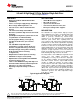
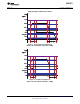
VDD
IN-
IN+
VREF
OUTH
OUTL
UCC27611
R1
R2
Q1
IN+
D1
C1
+
VOUT
VSOURCE
L1
C3
VREF
4.5 V to 18 V
Non-Inverting Input Inverting Input
C2
VDD
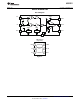
1
2
3
6
5
4
VDD
IN-
IN+
VREF
OUTH
OUTL
UCC27611
R1
R2
Q1
VREF
D1
C1
+
VOUT
VSOURCE
L1
C3
VREF
4.5 V to 18 V
C2
VDD
IN-
7
GND
7
GND
UCC27611
www.ti.com
SLUSBA5B –DECEMBER 2012
4-A and 6-A High-Speed 5-V Drive, Optimized Single-Gate Driver
Check for Samples: UCC27611
1
FEATURES
APPLICATIONS
• Enhancement Mode Gallium Nitride FETs • Switch-Mode Power Supplies
(eGANFETs)
• DC-to-DC Converters
• 4.0-V to 18-V Single Supply Range VDD Range
• Synchronous Rectification
• Drive Voltage VREF Regulated to 5 V
• Solar Inverters, Motor Control, UPS
• 4-A Peak Source and 6-A Peak Sink Drive
• Envelope Tracking Power Supplies
Current
• 1-Ω and 0.35-Ω Pull-Up and Pull-Down DESCRIPTION
Resistance (maximize high slew-rate dV and dt
The UCC27611 is a single-channel, high-speed, gate
immunity)
driver optimized for 5-V drive, specifically addressing
enhancement mode GaN FETs. The drive voltage
• Split Output Configuration (allows turn-on and
VREF is precisely controlled by internal linear
off optimization for individual FETs)
regulator to 5 V. The UCC27611 offers asymmetrical
• Fast Propagation Delays (14-ns typical)
rail-to-rail peak current drive capability with 4-A
• Fast Rise and Fall Times (9-ns and 4-ns
source and 6-A sink. Split output configuration allows
individual turn-on and off time optimization depending
typical)
on FET. Package and pinout with minimum parasitic
• TTL and CMOS Compatible Inputs
inductances reduce the rise and fall time and limit the
(independent of supply voltage allow easy
ringing. Additionally, the short propagation delay with
interface to digital and analog controllers)
minimized tolerances and variations allows efficient
• Dual Input Design offering Drive Flexibility
operation at high frequencies. The 2-Ω and 0.3-Ω
(both inverting and non-inverting
pull-up and pull-down resistance boosts immunity to
hard switching with high slew rate dV and dt.
configurations)
• Output Held Low when Inputs are Floating
The independence from VDD input signal thresholds
ensure TTL and CMOS low-voltage logic
• VDD Under Voltage Lockout (UVLO)
compatibility. For safety reason when the input pins
• Optimized Pinout Compatible with eGANFET
are in a floating condition, the internal input pull-up
Footprint for Easy Layout
and down resistors hold the output LOW. Internal
• 2 mm x 2 mm WSON-6 Package with Exposed
circuitry on VREF pin provides an under voltage
Thermal and Ground Pad, (minimized parasitic
lockout function that holds output LOW until VREF
supply voltage is within operating range. UCC27611
inductances to reduce gate ringing)
is offered in a small 2 mm x 2 mm WSON-6 package
• Operating Temperature Range of -40°C to
(DRV) with exposed thermal and ground pad which
140°C
improves the package power handling capability. The
UCC27611 operates over wide temperature range
from -40°C to 140°C.
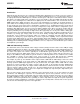
Typical Application Diagram
1
Please be aware that an important notice concerning availability, standard warranty, and use in critical applications of
Texas Instruments semiconductor products and disclaimers thereto appears at the end of this data sheet.
PRODUCTION DATA information is current as of publication date.
Copyright © 2012, Texas Instruments Incorporated
Products conform to specifications per the terms of the Texas
Instruments standard warranty. Production processing does not
necessarily include testing of all parameters.