UCC28070A www.ti.
UCC28070A SLUSAW0 – MARCH 2012 www.ti.com DESCRIPTION (CONT.) Like UCC28070, UCC28070A also features multiple innovations including current synthesis and quantized voltage feed-forward to promote performance enhancements in PF, efficiency, THD, and transient response. Features including frequency dithering, clock synchronization, and slew rate enhancement further expand the potential performance enhancements.
UCC28070A www.ti.com SLUSAW0 – MARCH 2012 ELECTROSTATIC DISCHARGE (ESD) PROTECTION RATING Human Body Model (HBM) 2,000 Charged Device Model (CDM) 500 UNIT V RECOMMENDED OPERATING CONDITIONS over operating free-air temperature range (unless otherwise noted) PARAMETER MIN VCC Input Voltage (from a low-impedance source) MAX VUVLO + 1 V VREF Load Current UNIT 21 V 2 mA VINAC Input Voltage Range 0 3 IMO Voltage Range 0 3.3 PKLMT, CSA, & CSB Voltage Range 0 3.
UCC28070A SLUSAW0 – MARCH 2012 www.ti.com ELECTRICAL CHARACTERISTICS over operating free-air temperature range −40°C < TA < 125°C, TJ = TA, VCC = 12 V, GND = 0 V, RRT = 75 kΩ, RDMX = 68.1 kΩ, RRDM = RSYN = 100 kΩ, CCDR = 2.2 nF, CSS = CVREF = 0.
UCC28070A www.ti.com SLUSAW0 – MARCH 2012 ELECTRICAL CHARACTERISTICS (continued) over operating free-air temperature range −40°C < TA < 125°C, TJ = TA, VCC = 12 V, GND = 0 V, RRT = 75 kΩ, RDMX = 68.1 kΩ, RRDM = RSYN = 100 kΩ, CCDR = 2.2 nF, CSS = CVREF = 0.1 μF, CVCC = 1 μF, IVREF = 0 mA (unless otherwise noted) SYMBOL PARAMETER TEST CONDITIONS MIN TYP MAX UNITS Clock Synchronization VCDR SYNC enable threshold Measured at CDR (rising) 5 5.
UCC28070A SLUSAW0 – MARCH 2012 www.ti.com ELECTRICAL CHARACTERISTICS (continued) over operating free-air temperature range −40°C < TA < 125°C, TJ = TA, VCC = 12 V, GND = 0 V, RRT = 75 kΩ, RDMX = 68.1 kΩ, RRDM = RSYN = 100 kΩ, CCDR = 2.2 nF, CSS = CVREF = 0.
UCC28070A www.ti.com SLUSAW0 – MARCH 2012 ELECTRICAL CHARACTERISTICS (continued) over operating free-air temperature range −40°C < TA < 125°C, TJ = TA, VCC = 12 V, GND = 0 V, RRT = 75 kΩ, RDMX = 68.1 kΩ, RRDM = RSYN = 100 kΩ, CCDR = 2.2 nF, CSS = CVREF = 0.1 μF, CVCC = 1 μF, IVREF = 0 mA (unless otherwise noted) SYMBOL PARAMETER TEST CONDITIONS MIN TYP MAX UNITS Current Synthesizer VRSYNTH Regulation voltage Synthesizer disable threshold VSENSE = 3 V, VINAC = 0 V 2.91 3 3.
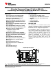
UCC28070A SLUSAW0 – MARCH 2012 www.ti.com DEVICE INFORMATION TSSOP-20 Top View, PW Package CDR 1 20 RDM 2 19 VAO 3 18 SS VSENSE 4 17 GDB VINAC DMAX RT 5 16 GND IMO 6 15 VCC RSYNTH 7 14 GDA CSB 8 13 VREF CSA 9 12 CAOA 10 11 CAOB PKLMT TERMINAL FUNCTIONS NAME CDR 8 PIN # 1 I/O DESCRIPTION I Dither Rate Capacitor. Frequency-dithering timing pin. An external capacitor to GND programs the rate of oscillator dither.
UCC28070A www.ti.com SLUSAW0 – MARCH 2012 TERMINAL FUNCTIONS (continued) NAME PIN # I/O DESCRIPTION CAOB 11 O Phase B Current Amplifier Output. Output of phase B’s transconductance current amplifier. Internally connected to the inverting input of phase B’s PWM comparator for trailing-edge modulation. Connect the current regulation loop compensation components between this pin and GND. CAOA 12 O Phase A Current Amplifier Output. Output of phase A’s transconductance current amplifier.
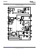
UCC28070A SLUSAW0 – MARCH 2012 www.ti.com Functional Block Diagram + OVP VCC 15 25V VREF 13 6V Linear EN Regulator 160 On o 140 Off C + ReStart ThermSD 0.75V 0.60V + R Q UVLO 10.2V 9.2V + S Q VSENSE GND 16 Ext.Disable SS 8V 0.75V 0.60V VSENSE 3.18V 3.08V Fault ZeroPwr + 0.90V 0.75V + VAO 6 IMO 5 VINAC DMAX 20 Voltage FeedForward CLKA Oscillator w/ Freq. Dither RT 19 CLKB IIMO = VVINAC * (VVAO – 1) KVFF OffA * 17uA 250nA KVFF x OffB Mult.
UCC28070A www.ti.com SLUSAW0 – MARCH 2012 TYPICAL CHARACTERISTICS SUPPLY CURRENT vs TEMPERATURE REFERENCE VOLTAGE vs TEMPERATURE 12 6.18 6.12 IVCC, VCC = 12 V, enabled VREF - Reference Voltage - V IVCC - Supply Current - mA 10 8 IVCC, VCC = 12 V, disabled 6 4 6.06 VREF (IVREF = 0 mA) 6.00 5.94 2 5.88 0 5.82 -60 -40 -20 0 20 40 60 80 100 120 140 -60 -10 TJ - Temperature - 0C 40 90 140 TJ - Temperature - 0C Figure 1. Figure 2.
UCC28070A SLUSAW0 – MARCH 2012 www.ti.com TYPICAL CHARACTERISTICS (continued) MULTIPLIER OUTPUT CURRENT vs VOLTAGE AMPLIFIER OUTPUT MULTIPIER CONSTANT vs TEMPERATURE 180 20 QVFF Level Level 1 19 Level 2 140 Level 3 120 Multiplier Constant - mA IMO - Multiplier Output Current - mA 160 Level 4 Level 5 100 Level 6 80 Level 7 Level 8 60 18 VAO = 3.0 V VAO = 5.0 V 17 16 VAO = 1.5 V 40 15 VAO = 1.
UCC28070A www.ti.com SLUSAW0 – MARCH 2012 TYPICAL CHARACTERISTICS (continued) VOLTAGE AMPLIFIER TRANSFER FUNCTION vs VSENSE VOLTAGE AMPLIFIER TRANSCONDUCTANCE vs TEMPERATURE 40 IVAO - Voltage Amplifier Output Current - mA VAO - Voltage Amplifier Transconductance - mS 80 75 70 65 60 55 50 20 0 -20 -40 -60 -80 -100 -120 -140 -60 -40 -20 0 20 60 40 80 100 120 140 2.6 2.5 2.7 2.8 2.9 TJ - Temperature - 0C 3.0 3.1 3.2 3.3 3.4 3.5 VSENSE - V Figure 9. Figure 10.
UCC28070A SLUSAW0 – MARCH 2012 www.ti.com TYPICAL CHARACTERISTICS (continued) CAx INPUT OFFSET VOLTAGE vs TEMPERATURE (at 0.8 V common mode) CA1 TO CA2 RELATIVE OFFSET vs TEMPERATURE (at 0.8 V common mode) 5 CAx +3s 0 CAx Input Offset - mV CA1 to CA2 Relative Offset Voltage - mV 15 -5 CAx AVG -10 CAx -3s -15 -20 10 A-B +3s 5 0 A-B AVG -5 A-B -3s -10 -15 -60 -40 -20 0 20 40 60 80 100 120 140 -60 -40 -20 TJ - Temperature - 0C 40 60 80 100 120 140 Figure 12. Figure 13.
UCC28070A www.ti.com SLUSAW0 – MARCH 2012 TYPICAL CHARACTERISTICS (continued) CAx INPUT OFFSET VOLTAGE vs TEMPERATURE (at 3.6 V common mode) CA1 TO CA2 RELATIVE OFFSET vs TEMPERATURE (at 3.
UCC28070A SLUSAW0 – MARCH 2012 www.ti.com APPLICATION INFORMATION THEORY OF OPERATION Interleaving One of the main benefits from the 180° interleaving of phases is significant reductions in the high-frequency ripple components of both the input current and the current into the output capacitor of the PFC pre-regulator.
UCC28070A www.ti.com SLUSAW0 – MARCH 2012 Programming the PWM Frequency and Maximum Duty-Cycle Clamp The PWM frequency and maximum duty-cycle clamps for both GDx outputs of the UCC28070A are set through the selection of the resistors connected to the RT and DMAX pins, respectively. The selection of the RT resistor (RRT) directly sets the PWM frequency (fPWM). RRT (k W ) = 7500 f PWM (kHz ) (3) Once RRT has been determined, the DMAX resistor (RDMX) may be derived.
UCC28070A SLUSAW0 – MARCH 2012 www.ti.com External Clock Synchronization The UCC28070A has also been designed to be easily synchronized to almost any external frequency source. By disabling frequency dithering (pulling CDR > 5 V), the UCC28070A’s SYNC circuitry is enabled permitting the internal oscillator to be synchronized with pulses presented on the RDM pin.
UCC28070A www.ti.com SLUSAW0 – MARCH 2012 Multi-phase Operation External synchronization also facilitates using more than 2 phases for interleaving. Multiple UCC28070As can easily be paralleled to add an even number of additional phases for higher-power applications. With appropriate phase-shifting of the synchronization signals, even more input and output ripple current cancellation can be obtained. (An odd number of phases can be accommodated if desired, but the ripple cancellation would not be optimal.
UCC28070A SLUSAW0 – MARCH 2012 www.ti.
UCC28070A www.ti.com SLUSAW0 – MARCH 2012 Current Synthesizer One of the most prominent innovations in the UCC28070A design is the current synthesizer circuitry that synchronously monitors the instantaneous inductor current through a combination of on-time sampling and offtime down-slope emulation. During the on-time of the GDA and GDB outputs, the inductor current is recorded at the CSA and CSB pins respectively via the current transformer network in each output phase.
UCC28070A SLUSAW0 – MARCH 2012 www.ti.com Programmable Peak Current Limit The UCC28070A has been designed with a programmable cycle-by-cycle peak current limit dedicated to disabling either GDA or GDB output whenever the corresponding current-sense input (CSA or CSB respectively) rises above the voltage established on the PKLMT pin. Once an output has been disabled via the detection of peak current limit, the output remains disabled until the next clock cycle initiates a new PWM period.
UCC28070A www.ti.com SLUSAW0 – MARCH 2012 Linear Multiplier The multiplier of the UCC28070A generates a reference current which represents the desired wave shape and proportional amplitude of the ac input current. This current is converted to a reference voltage signal by the RIMO resistor, which is scaled in value to match the voltage of the current-sense signals. The instantaneous multiplier current is dependent upon the rectified, scaled input voltage VVINAC and the voltage-error amplifier output VVAO.
UCC28070A SLUSAW0 – MARCH 2012 www.ti.com The multiplier output current IIMO for any line and load condition can thus be determined by the equation I IMO = 17 m A ´ (VVINAC )´ (VVAO - 1) kVFF (13) 2 Because the kVFF value represents the scaled VRMS at the center of a level, VVAO will adjust slightly upwards or downwards when VINACpk is either lower or higher than the center of the QVFF voltage range to compensate for the difference.
UCC28070A www.ti.com SLUSAW0 – MARCH 2012 This IIN(pk) value represents the combined average current through the boost inductors at the peak of the line voltage. Each inductor current is detected and scaled by a current-sense transformer (CT).
UCC28070A SLUSAW0 – MARCH 2012 www.ti.com Enhanced Transient Response (VA Slew-Rate Correction) Due to the low voltage loop bandwidth required to maintain proper PFC and ignore the slight 120-Hz ripple on the output, the response of ordinary controllers to input voltage and load transients will also be slow. However, the QVFF function effectively handles the line transient response with the exception of any minor adjustments needed within a QVFF level.
UCC28070A www.ti.com SLUSAW0 – MARCH 2012 Adaptive Soft Start In order to maintain a controlled power up, the UCC28070A has been designed with an adaptive soft-start function that overrides the internal reference voltage with a controlled voltage ramp during power up. On initial power up, once VVSENSE exceeds the 0.75-V enable threshold (VEN), the internal pull down on the SS pin is released, and the 1.5-mA adaptive soft-start current source is activated. This 1.
UCC28070A SLUSAW0 – MARCH 2012 www.ti.com PFC Start-Up Hold Off An additional feature designed into the UCC28070A is the “Start-Up Hold Off” logic that prevents the device from initiating a soft-start cycle until the VAO is below the zero-power threshold (0.75 V). This feature ensures that the SS cycle will initiate from zero-power and zero duty-cycle while preventing the potential for any significant inrush currents due to stored charge in the VAO compensation network.
UCC28070A www.ti.com SLUSAW0 – MARCH 2012 Current Loop Compensation The UCC28070A incorporates two identical and independent transconductance-type current-error amplifiers (one for each phase) with which to control the shaping of the PFC input current waveform. The current-error amplifier (CA) forms the heart of the embedded current control loop of the boost PFC pre-regulator, and is compensated for loop stability using familiar principles [4, 5].
UCC28070A SLUSAW0 – MARCH 2012 www.ti.com The switching ripple voltage should be attenuated to less than 1/10 of the ΔVRMP amplitude so as to be considered “negligible” ripple. Thus, CAOx gain at fPWM is: DVRMP ´ k SYNC g mc Rzc £ DI LB ´ RS 10 N CT (23) where ∆ILB is the maximum peak-to-peak ripple current in the boost inductor, and gmc is the transconductance of the CA, 100 μS.
UCC28070A www.ti.com SLUSAW0 – MARCH 2012 Voltage Loop Compensation The outer voltage control loop of the dual-phase PFC controller functions the same as with a single-phase controller, and compensation techniques for loop stability are standard [4]. The bandwidth of the voltage-loop must be considerably lower than the twice-line ripple frequency (f2LF) on the output capacitor, to avoid distortioncausing correction to the output voltage.
UCC28070A SLUSAW0 – MARCH 2012 www.ti.com The output capacitor maximum low-frequency zero-to-peak ripple voltage is closely approximated by: v0 pk = Pinavg ´ X Cout Voutavg Pinavg = Voutavg ´ 2p ´ f 2 LF ´ Cout (27) where PIN(avg) is the total maximum input power of the interleaved-PFC pre-regulator, VOUT(avg) is the average output voltage and COUT is the output capacitance. VSENSEpk = vopkxkR, where kR is the gain of the resistor-divider network on VSENSE.
UCC28070A www.ti.com SLUSAW0 – MARCH 2012 Advanced Design Techniques Current Loop Feedback Configuration (Sizing of the Current Transformer Turns Ratio and Sense Resistor (RS) A current-sense transformer (CT) is typically used in high-power applications to sense inductor current while avoiding significant losses in the sensing resistor. For average current-mode control, the entire inductor current waveform is required; however low-frequency CTs are obviously impracticable.
UCC28070A SLUSAW0 – MARCH 2012 www.ti.com In general, 50 ≤ NCT ≤ 200 is a reasonable range from which to choose. If NCT is too low, there may be high power loss in RS and insufficient LM. If too high, there could be excessive LLK and Cd. (A one-turn primary winding is assumed.) LLK IDS 1 NCT LM iM CSx RSER D Cd Reset Network RS Figure 24.
UCC28070A www.ti.com SLUSAW0 – MARCH 2012 It is vital that the CT has plenty of Vμs design-margin to accommodate various special situations where there to be several consecutive maximum duty-cycle periods at maximum input current, such as during peak current limiting.
UCC28070A SLUSAW0 – MARCH 2012 www.ti.com Current Sense Offset and PWM Ramp for Improved Noise Immunity To improve noise immunity at extremely light loads, a PWM ramp with a dc offset is recommended to be added to the current sense signals. Electrical components RTA, RTB, ROA, ROB, CTA, CTB, DPA1, DPA2, DPB1, DPB1 CTA, CTB form a PWM ramp that is activated and deactivated by the gate drive outputs of the UCC28070A. Resistor ROA and ROB add a dc offset to the CS resistors (RSA and RSB).
UCC28070A www.ti.com SLUSAW0 – MARCH 2012 When the inductor current becomes discontinuous the boost inductors ring with the parasitic capacitances in the boost stages. This inductor current rings through the CTs causing a false current sense signal. Please refer to the following graphical representation of what the current sense signal looks like when the inductor current goes discontinuous.
UCC28070A SLUSAW0 – MARCH 2012 www.ti.com Recommended PCB Device Layout Interleaved PFC techniques dramatically reduce input and output ripple current caused by the PFC boost inductor, which allows the circuit to use smaller and less expensive filters. To maximize the benefits of interleaving, the output filter capacitor should be located after the two phases allowing the current of each phase to be combined together before entering the boost capacitor.
PACKAGE OPTION ADDENDUM www.ti.
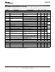
PACKAGE MATERIALS INFORMATION www.ti.com 14-Jul-2012 TAPE AND REEL INFORMATION *All dimensions are nominal Device UCC28070APWR Package Package Pins Type Drawing TSSOP PW 20 SPQ Reel Reel A0 Diameter Width (mm) (mm) W1 (mm) 2000 330.0 16.4 Pack Materials-Page 1 6.95 B0 (mm) K0 (mm) P1 (mm) 7.1 1.6 8.0 W Pin1 (mm) Quadrant 16.
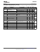
PACKAGE MATERIALS INFORMATION www.ti.com 14-Jul-2012 *All dimensions are nominal Device Package Type Package Drawing Pins SPQ Length (mm) Width (mm) Height (mm) UCC28070APWR TSSOP PW 20 2000 367.0 367.0 38.
IMPORTANT NOTICE Texas Instruments Incorporated and its subsidiaries (TI) reserve the right to make corrections, enhancements, improvements and other changes to its semiconductor products and services per JESD46C and to discontinue any product or service per JESD48B. Buyers should obtain the latest relevant information before placing orders and should verify that such information is current and complete.