
Datasheet


SLUS456D − APRIL 1999 - REVISED AUGUST 2002
1
www.ti.com
D Dual Output Drive Stages in Push-Pull
Configuration
D Current Sense Discharge Transistor to
Improve Dynamic Response
D 130-µA Typical Starting Current
D 1-mA Typical Run Current
D Operation to 1 MHz
D Internal Soft Start
D On-Chip Error Amplifier With 2-MHz Gain
Bandwidth Product
D On Chip VDD Clamping
D Output Drive Stages Capable of 500-mA
Peak-Source Current, 1-A Peak-Sink Current
description
The UCC3808A is a family of BiCMOS push-pull, high-speed, low-power, pulse-width modulators. The UCC3808A
contains all of the control and drive circuitry required for off-line or dc-to-dc fixed frequency current-mode switching
power supplies with minimal external parts count.
The UCC3808A dual output drive stages are arranged in a push-pull configuration. Both outputs switch at half the
oscillator frequency using a toggle flip-flop. The dead time between the two outputs is typically 60 ns to 200 ns
depending on the values of the timing capacitor and resistors, thus limiting each output stage duty cycle to less than
50%.
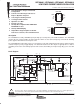
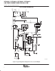
block diagram
UDG-00097
Note: Pinout shown is for SOIC and PDIP packages. TSSOP pinout is different.
312
8
7
6
5
4
OSCILLATOR
S
Q
R
RC
1.2R
R
0.5 V
PEAK CURRENT
COMPARATOR
Q
Q
T
S
Q
R
S
Q
R
VDD
VOLTAGE
REFERENCE
14 V
PWM
COMPARATOR
PWM
LATCH
SOFT START
0.5 V
VDD−1 V
0.75 V
2.2 V
2.0 V
FB COMP CS
VDD
OUTA
OUTB
GND
SLOPE = 1 V/ms
VDD OK
OVERCURRENT
COMPARATOR
22 k
Ω
Copyright 2002, Texas Instruments Incorporated
! " #$%! " &$'(#! )!%*
)$#!" # ! "&%##!" &% !+% !%" %," "!$%!"
"!)) -!.* )$#! &#%""/ )%" ! %#%""(. #($)%
!%"!/ (( &%!%"*
Please be aware that an important notice concerning availability, standard warranty, and use in critical applications of
Texas Instruments semiconductor products and disclaimers thereto appears at the end of this data sheet.
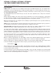
1
2
3
4
8
7
6
5
COMP
FB
CS
RC
VDD
OUTA
OUTB
GND
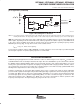
D OR N PACKAGE
(TOP VIEW)
1
2
3
4
8
7
6
5
OUTA
VDD
COMP
FB
OUTB
GND
RC
CS
PW PACKAGE
(TOP VIEW)