
Datasheet

UCC284–5, UCC284–12, UCC284–ADJ, UCC384–5, UCC384–12, UCC384–ADJ
LOW-DROPOUT 0.5-A NEGATIVE LINEAR REGULATOR
SLUS234D – JANUARY 2000 – REVISED FEBRUARY 2002
1
POST OFFICE BOX 655303 • DALLAS, TEXAS 75265
D Precision Negative Series Pass Voltage
Regulation
D 0.2 V Dropout at 0.5 A
D Wide Input Voltage Range –3.2 V to –15 V
D Low Quiescent Current Irrespective of Load
D Simple Logic Shutdown Interfacing
D –5 V, –12 V, and Adjustable Output
D 2.5% Duty Cycle Short Circuit Protection
description
The UCC384-x family of negative linear-series pass regulators is tailored for low-dropout applications where
low-quiescent power is important. Fabricated with a BCDMOS technology ideally suited for low input-to-output
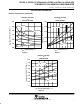
differential applications, the UCC384-x passes 0.5 A while requiring only 0.2 V of input-voltage headroom.
Dropout voltage decreases linearly with output current, so that dropout at 50 mA is less than 20 mV.
Quiescent current consumption for the device under normal (non-dropout) conditions is typically 200 µA. An
integrated charge pump is internally enabled only when the device is operating near dropout with low VIN. This
ensured that the device meets the dropout specifications even for maximum load current and a VIN of –3.2 V
with only a modest increase in quiescent current. Quiescent current is always less than 350 µA, with the charge
pump enabled. The quiescent current of the UCC384 does not increase with load current.
Short-circuit current is internally limited. The device responds to a sustained overcurrent condition by turning
off after a t
ON
delay. The device then stays off for a period, t
OFF
, that is 40 times the t
ON
delay. The device then
begins pulsing on and off at the t
ON
/t
OFF
duty cycle of 2.5%. This drastically reduces the power dissipation during
short circuit such that heat sinking, if at all required, must only accommodate normal operation. An external
capacitor sets the on time. The off time is always 40 times t
ON
.
The UCCx84-x can be shutdown to 45 µA (maximum) by pulling the SD/CT pin more positive than –0.7 V. To
allow for simpler interfacing, the SD/CT pin may be pulled up to 6 V above the ground pin without turning on
clamping diodes.
Internal power dissipation is further controlled with thermal-overload protection circuitry. Thermal shutdown
occurs if the junction temperature exceeds 140°C. The chip remains off until the temperature has dropped 20°C
(T
J
= 120°C).
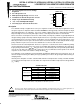
AVAILABLE OPTIONS
T
A
OUTPUT VOLTAGE (V) PACKAGE DEVICES
T
A
TYP (SOIC) DP
–5 UCC284DP–5
–40°C to 85°C
–12 UCC284DP–12
40 C
to
85 C
ADJ UCC284DP–ADJ
–5 UCC384DP–5
0°C to 70°C
–12 UCC384DP–12
ADJ UCC384DP–ADJ
†
All package types are available taped and reeled. Add TR suffix to device type
(e.g. UCC284DP–5TR) to order quantities of 3000 devices per reel.
Copyright 2000, Texas Instruments Incorporated
PRODUCTION DATA information is current as of publication date.
Products conform to specifications per the terms of Texas Instruments
standard warranty. Production processing does not necessarily include
testing of all parameters.
Please be aware that an important notice concerning availability, standard warranty, and use in critical applications of
Texas Instruments semiconductor products and disclaimers thereto appears at the end of this data sheet.
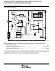
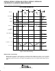
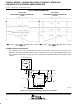
DP PACKAGE
(FRONT VIEW)
VIN
VIN
SD/CT
VOUT
VIN
VOUTS
VIN
GND
1
2
3
4
8
7
6
5