
Datasheet

SLUS517C − DECEMBER 2002 − REVISED SEPTEMBER 2005
2
www.ti.com
DESCRIPTION (CONTINUED)
The transient response of the circuit is enhanced by allowing a much faster charge/discharge of the voltage
amplifier output capacitance when the output voltage falls outside a certain regulation window. A number of
additional features such as UVLO circuit with selectable hysteresis levels, an accurate reference voltage for the
voltage amplifier, zero power detect, OVP/enable, peak current limit, power limiting, high-current output gate
driver characterize the PFC section.
The PWM section features peak current mode control (with a ramp signal available to add slope compensation),
programmable soft-start, accurate maximum duty cycle clamp, peak current limit and high-current output gate
driver. The oscillator for the combination controller is available in two versions. In UCC28510, UCC28511,
UCC28512, and UCC28513, the PWM and the PFC circuits are switched at the same frequency. In the
UCC28514, UCC28515, UCC28516, and UCC28517, the PWM stage frequency is twice that of the PFC
frequency. The PWM stage is suppressed until the PFC output has reached 90% of its programmed value during
startup. During line dropout and turn off, the device allows the PWM stage to operate until the PFC output has
dropped to 47% (UCC28512, UCC28513, UCC28516, and UCC28517) or 71% (UCC28510, UCC28511,
UCC28514, and UCC28515) of its nominal value. See available options table on page 1 for a summary of
options.
The UCC28510 family also features leading-edge modulation for the PFC stage and trailing-edge modulation
for the PWM stage in order to reduce the ripple current in the boost output capacitor. The current amplifier
implementation associated with this scheme also results in better noise immunity.
Available in 20-pin N and DW packages.
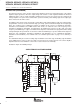
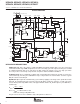
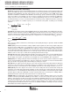
SIMPLIFIED APPLICATION DIAGRAM
12
3
16
18
10
5
7
2
UCC2851X
GT1
VSENSE
ISENSE1
IAC
GT2
VREF
VERR
RT
+
−
D1
VAC
15
14
13
11
17
19
20
PWRGND
VAOUT 1
6
VFF
MOUT
CAOUT
PKLMT
SS2 8
9
D_MAX
CT_BUFF
GND
ISENSE2
VCC
REF
PRIMARY SECONDARY
+
−
VOUT
+
4
REF
BIAS
RECT
+
−
PWM
V−LOOP
Z
Z
Z