
Datasheet

SLUS517C − DECEMBER 2002 − REVISED SEPTEMBER 2005
7
www.ti.com
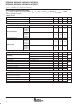
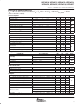
ELECTRICAL CHARACTERISTICS
T
A
= –40°C to 105°C for the UCC2851x, T
A
= T
J
, VCC = 12 V, R
T
= 156 kΩ, R
CT_BUFF
= 10 kΩ
(unless otherwise noted)
PWM stage overcurrent limit
PARAMETER TEST CONDITIONS MIN TYP MAX UNITS
Peak current comparator threshold voltage 1.15 1.30 1.45 V
Input bias current
(1)
50 nA
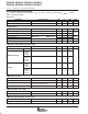
PWM stage gate driver
PARAMETER TEST CONDITIONS MIN TYP MAX UNITS
GT2 pull-up resistance −100 mA ≤ ∆I
OUT
≤ −200 mA 5 12 Ω
GT2 pull-down resistance I
OUT
= 100 mA 2 10 Ω
GT2 output rise time
C
LOAD
= 1 nF, R
LOAD
= 10 Ω
16 25 ns
GT2 output fall time
C
LOAD
= 1 nF, R
LOAD
= 10 Ω
7 15 ns
1. Ensured by design. Not 100% tested in production.
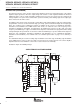
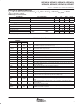
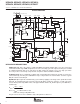
TERMINAL FUNCTIONS
TERMINAL
I/O
DESCRIPTION
NAME NO. Stage
I/O
DESCRIPTION
CAOUT
15 PFC O
Output of the current control amplifier of the PFC stage. CAOUT is internally connected
to the PWM comparator input in the PFC stage
CT_BUFF 5 PWM O
Internally buffered PWM stage oscillator ramp output, typically used to program slope
compensation with a single resistor
D_MAX 4 PWM I Positive input to set the maximum duty cycle clamp level of the PWM stage
GND 6 − − Analog ground
GT1 12 PFC O PFC stage gate drive output
GT2 10 PWM O PWM stage gate drive output
IAC 18 PFC I Multiplier current input that is proportional to the instantaneous rectified line voltage
ISENSE1 16 PFC I Non-inverting input to the PFC stage current amplifier
ISENSE2 8 PWM I Input for PWM stage current sense and peak current limit
MOUT 17 PFC I/O
PFC multiplier high−impedance current output, internally connected to the current am-
plifier inverting input
PKLMT 14 PFC I Voltage input to the PFC peak current limit comparator
PWRGND 11 − − Power ground for GT1, GT2 and high current return paths
RT 2 − I Oscillator programming pin that is set with a single resistor to GND
SS2 13 PWM I Soft start for the PWM stage
VAOUT 1 PFC I/O
Output of the PFC transconductance voltage amplifier and it is internally connected to
the Zero Power Detect comparator input and the multiplier input
VCC 9 − I Positive supply voltage pin
VERR 7 PWM I
Feedback error voltage input for the PWM stage, typically connected to an optocoupler
output
VFF 19 PFC I
Voltage feedforward pin for the PFC stage, sources an IAC/2 current that should be
externally filtered
VREF 20 − O Precision 7.5-V reference output
VSENSE 3 PFC I
Inverting input to the PFC transconductance voltage amplifier, and input to the OVP,
ENABLE and UVLO2 comparators