
Datasheet

SLUS517C − DECEMBER 2002 − REVISED SEPTEMBER 2005
8
www.ti.com
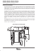
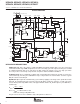
BLOCK DIAGRAM
VREF20
14
12
11
9
17
16
GT1
PWRGND
ISENSE1
VCC
VAOUT
1.9 V
PKLMT
7.5 V
REFERENCE
UVLO
16 V, 9.7 V
10.2 V, 9.7 V
VCC
15
Q
S
CAOUT
SS2
g
M
VOLTAGE
ERROR AMP
8.0 V
13
1
3VSENSE
VFF
19
IAC
18
MOUT
MIRROR
2:1
7.5 V
ENABLE
PFCOVP
÷
X
X
MULT
CLK1
CURRENT
AMP
6.75 V
GND
10 GT2
VCC
8
CLK2
1.5 V
1.3 V
R
I
LIMIT
VERR ISENSE2
I
LIMIT
S
Q
UVLO2
PWM
0.33 V
(V
FF
)
2
ZERO
POWER
PWM STAGE
SOFT START
+
PWM
+
+
+
+
+
7
6
OSC
CLK2
CLK1
+
+
PWM
+
+
PFC
CLK1 CLK2
2RT
+
D_MAX
4
CT_BUFF
5
D_MAX
COMP
3 V
+
R
R
R
PWM
PFC
PWM
PFC
I
RT
PFC:PWM
Frequency
1:1 = I
RT
1:2 = 0.5I
RT
1x:2x Option Only
DETAILED PIN DESCRIPTIONS
CAOUT (Pin 15): This is the output of a wide-bandwidth operational amplifier that senses line current and
commands the PFC stage PWM comparator to force the correct duty cycle. This output can swing close to GND
to command maximum duty cycle, and above the PFC ramp peak voltage to force zero duty cycle when
necessary. Connect current loop compensation components between CAOUT and MOUT.
CT_BUFF (Pin 5): The 4-V amplitude oscillator ramp is internally buffered at this pin to allow a resistor to be
connected directly from this pin to ISENSE2 for slope compensation. The internal buffer can drive a typical
500-µA resistive load at this pin.
D_MAX (Pin 4): Program the maximum duty cycle at GT2 by applying a dc voltage to this pin. Between 0.09
and 0.90, the maximum duty ratio is linearly related to D_MAX. Usually, this voltage is set with a precision
resistor divider powered by VREF. A first order approximation, with the CT_BUFF frequency near 200 kHz, is
estimated by:
D
MAX
^
V
DX
* 1.15 V
4V
where, D
MAX
is a dimensionless ratio
V
DX
is the voltage at D_MAX in volts
This pin can also be used to set D
MAX
to 0 by setting V
DX
less than 0.7 V.