
Datasheet

SLUS517C − DECEMBER 2002 − REVISED SEPTEMBER 2005
9
www.ti.com
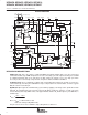
DETAILED PIN DESCRIPTIONS (CONTINUED)
GND (Pin 6): Signal ground for the integrated circuit. All voltages measured with respect to ground are
referenced to this pin. The bypass capacitors for VCC and VREF should connect to this pin with as little lead
length as possible. PWRGND must be externally connected to this pin. For best results, use a single small circuit
trace to electrically connect between the circuits that use the GND return path and the circuits that use the
PWRGND return path.
GT1 (Pin 12): A 2-A peak source and 3-A peak sink current totem pole MOSFET gate driver for the PFC stage.
Some overshoot at GT1 can be expected when driving a capacitive load, but adding a minimal series resistor
of about 2 Ω between GT1 and the external MOSFET gate can reduce this overshoot. GT1 is disabled unless
VCC is outside the UVLO region and VREF is on.
GT2 (Pin 10): A 2-A peak source and 3-A peak sink current totem pole MOSFET gate driver for the PWM stage,
identical to the driver at GT1.
IAC (Pin 18): This multiplier input senses the rectified ac line voltage. A resistor between IAC and the line
voltage converts the instantaneous line voltage waveform into a current input for the analog multiplier. The
recommended maximum IAC current is 500 µA.
ISENSE1 (Pin 16): This pin is the non-inverting input terminal of the current amplifier. Connect a resistor
between this pin and the grounded side of the PFC stage current sensing resistor. The resistor connected to
this pin should have a value that equals the value of the resistor that is connected between the MOUT pin and
the ungrounded side of the PFC current sense resistor.
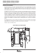
ISENSE2 (Pin 8): A voltage across the PWM stage external current sense resistor generates the input signal
to this pin, with the peak limit threshold set to 1.3 V for peak current mode control. An internal 1.5-V level shift
between ISENSE2 and the input to the PWM comparator provides greater noise immunity. The oscillator ramp
can also be summed into this pin for slope compensation. Figure 36 shows the typical relationship of the
capacitance on the ISENSE2 pin and the minimum controllable limit of the pulse width on the gate2 output. If
the V
ERR
is at the voltage that corresponds to a minimum controllable duty cycle and then is reduced further
the pulse width collapses to near zero.
MOUT (Pin 17): The output of the multiplier and the input to the current amplifier in the PFC stage are internally
connected at this pin. Set the power range of the PFC stage with a resistor tied between the MOUT pin and the
non-grounded end of the PFC current sense resistor. Connect impedance between the MOUT pin and the
CAOUT pin to compensate the PFC current control loop. The multiplier output is a current and the current
amplifier input is high impedance. The multiplier output current is given by:
I
MOUT
+
ǒ
V
VAOUT
* 1.0
Ǔ
I
IAC
K
ǒ
V
VFF
Ǔ
2
where, K is the multiplier gain constant, in volts
−1
.
PKLMT (Pin 14): Program the peak current limit of the PFC stage using this pin. The threshold for peak limit
is 0 V. Use a resistor divider between VREF and the non-grounded side of the PFC current sense resistor in
order to shift the level of this signal to a voltage that corresponds to the desired overcurrent threshold voltage,
measured across the PFC current sense resistor.
PWRGND (Pin 11): Ground for the output drivers at GT1 and GT2. This ground should be tied to GND externally
via a single Kelvin connection.