
Datasheet
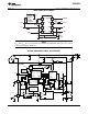

UCC28600
SLUS646J –NOVEMBER 2005– REVISED JULY 2011
www.ti.com
DESCRIPTION (CONT.)
The Design Calculator, (Texas Instruments Literature number SLVC104), located in the Tools and Software
section of the UCC28600 product folder, provides a user-interactive iterative process for selecting recommended
component values for an optimal design.
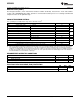
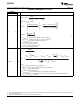
ABSOLUTE MAXIMUM RATINGS
over operating free-air temperature range unless otherwise noted
(1)
UCC28600 UNIT
VDD Supply voltage range I
DD
< 20 mA 32 V
I
DD
Supply current 20 mA
I
OUT(sink)
Output sink current (peak) 1.2
A
I
OUT(source)
Output source current (peak) -0.8
Analog inputs FB, CS, SS -0.3 to 6.0
V
V
OVP
-1.0 to 6.0
I
OVP(source)
-1.0 mA
V
STATUS
VDD = 0 V to 30 V 30 V
Power dissipation SOIC-8 package, T
A
= 25°C 650 mW
T
J
Operating junction temperature range –55 to 150
T
stg
Storage temperature –65 to 150 °C
T
LEAD
Lead temperature 1,6 mm (1/16 inch) from case for 10 seconds 300
(1) Stresses beyond those listed under “absolute maximum ratings” may cause permanent damage to the device. These are stress ratings
only, and functional operation of the device at these or any other conditions beyond those indicated under “recommended operating
conditions” is not implied. Exposure to absolute-maximum-rated conditions for extended periods may affect device reliability. All voltages
are with respect to GND. Currents are positive into, negative out of the specified terminal. Consult Packaging Section of the databook
for thermal limitations and considerations of packages.
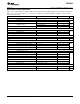
RECOMMENDED OPERATING CONDITIONS
MIN NOM MAX UNIT
VDD Input voltage 21 V
I
OUT
Output sink current 0 A
T
J
Operating junction temperature -40 105 °C
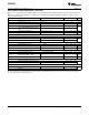
ELECTROSTATIC DISCHARGE (ESD) PROTECTION
MIN MAX UNIT
Human body model 2000
V
CDM 1500
2 Copyright © 2005–2011, Texas Instruments Incorporated