
Datasheet

1
2
3
4
8
7
6
5
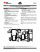
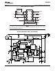
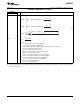
SS
FB
CS
GND
STATUS
OVP
VDD
OUT
UCC28600
D PACKAGE
(TOP VIEW)
UCC28600
SLUS646J –NOVEMBER 2005– REVISED JULY 2011
www.ti.com
ORDERING INFORMATION
T
A
PACKAGES PART NUMBER
-40°C to 105°C SOIC (D)
(1)
UCC28600D
(1) SOIC (D) package is available taped and reeled by adding “R” to the above part numbers. Reeled quantities for UCC28600DR is 2,500
devices per reel.
DEVICE INFORMATION
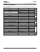
TERMINAL FUNCTIONS
TERMINAL
I/O DESCRIPTION
NAME NO.
Current sense input. Also programs power limit, and used to control modulation and activate overcurrent
CS 3 I protection. The CS voltage input originates across a current sense resistor and ground. Power limit is
programmed with an effective series resistance between this pin and the current sense resistor.
Feedback input or control input from the optocoupler to the PWM comparator used to control the peak current
in the power MOSFET. An internal 20-kΩ resistor is between this pin and the internal 5-V regulated voltage.
FB 2 I Connect the collector of the photo-transistor of the feedback optocoupler directly to this pin; connect the emitter
of the photo-transistor to GND. The voltage of this pin controls the mode of operation in one of the three
modes: quasi resonant (QR), frequency foldback mode (FFM) and green mode (GM).
Ground for internal circuitry. Connect a ceramic 0.1-μF bypass capacitor between VDD and GND, with the
GND 4 -
capacitor as close to these two pins as possible.
1-A sink (TrueDrive™ ) and 0.75-A source gate drive output. This output drives the power MOSFET and
OUT 5 O
switches between GND and the lower of VDD or the 13-V internal output clamp.
Over voltage protection (OVP) input senses line-OVP, load-OVP and the resonant trough for QR turn-on.
OVP 7 I Detect line, load and resonant conditions using the primary bias winding of the transformer, adjust sensitivity
with resistors connected to this pin.
Soft-start programming pin. Program the soft-start rate with a capacitor to ground; the rate is determined by the
capacitance and the internal soft-start charge current. Placement of the soft-start capacitor is critical and should
SS 1 I be placed as close as possible to the SS pin and GND, keeping trace length to a minimum. All faults discharge
the SS pin to GND through an internal MOSFET with an R
DS(on)
of approximately 100 Ω. The internal modulator
comparator reacts to the lowest of the SS voltage, the internal FB voltage and the peak current limit.
ACTIVE HIGH open drain signal that indicates the device has entered standby mode. This pin can be used to
STATUS 8 O disable the PFC control circuit (high impedance = green mode). STATUS pin is high during UVLO, (VDD <
startup threshold), and softstart, (SS < FB).
Provides power to the device. Use a ceramic 0.1-μF by-pass capacitor for high-frequency filtering of the VDD
VDD 6 I pin, as described in the GND pin description. Operating energy is usually delivered from auxiliary winding. To
prevent hiccup operation during start-up, a larger energy storage cap is also needed between VDD and GND.
6 Copyright © 2005–2011, Texas Instruments Incorporated