
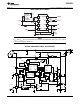
Datasheet

C
SS
u I
SS
t
SS(min)
(
due power limit
)
A
CS(FB)
ǒ
V
PL
* V
CS(os)
Ǔ
t
SS(min)
+
ȧ
ȧ
ȱ
Ȳ
* R
LOAD(ss)
C
OUT
2
ȏn
ȧ
ȡ
Ȣ
1 *
ǒ
V
OUT
* DV
OUT(step)
Ǔ
2
R
LOAD(ss)
P
OUT(max)limit
ȧ
ȣ
Ȥ
ȧ
ȧ
ȳ
ȴ
t
SS(min)
+
ȧ
ȱ
Ȳ
C
OUT
V
OUT
2
2 P
LIM
ȧ
ȳ
ȴ
R
ST2
+
V
BE(off)
I
STATUS(leakage)
R
ST1
+
R
ST2
ƪ
VDD
(uvlo*on)
* V
BE(sat)
* R
DS(on)
ǒ
I
CC
b
sat
Ǔ
ƫ
* R
DS(on)
V
BE(sat)
ǒ
ǒ
I
CC
b
sat
Ǔ
R
ST2
Ǔ
) V
BE(sat)
UCC28600
SLUS646J –NOVEMBER 2005– REVISED JULY 2011
www.ti.com
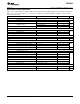
TERMINAL COMPONENTS (continued)
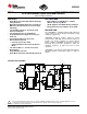
TERMINAL
I/O DESCRIPTION
(1) (2) (3)
NAME NO.
where t
SS(min)
is the greater of:
or
SS 1 I
(2)
• R
LOAD(ss)
is the effective load impedance during soft-start
(4)
• ΔV
OUT(step)
is the allowed change in V
OUT
due to a load step
(4)
• P
OUT(max limit)
Programmed power limit level, in W
(4)
• A
CS(FB)
is the current sense gain
(5)
• V
CS(os)
is the CS offset voltage
(5)
• I
SS
is the soft-start charging current
(5)
• V
PL
is the power limit threshold
(5)
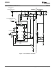
STATUS 8 O
where:
• β
SAT
is the gain of transistor Q
ST
in saturation
• V
BE(sat)
is the base-emitter voltage of transistor Q
ST
in saturation
• VDD
(uvlo-on)
is the startup threshold
(5)
• I
CC
is the collector current of Q
ST
• I
STATUS(leakage)
is the maximum leakage/off current of the STATUS pin
(5)
• V
BE(off)
is the maximum allowable voltage across the base emitter junction that will not turn Q
ST
on
• R
DS(on)
is the R
DS(on)
of STATUS
(5)
(4) Refer to the UCC28600 Design Calculator (TI Literature Number SLVC104) or laboratory measurements for currents, voltages and times
in the operational circuit.
(5) Refer to the Electrical Characteristics Table for constant parameters.
8 Copyright © 2005–2011, Texas Instruments Incorporated