
Datasheet

C
VDD
+
ƪ
ǒ
I
DD
) C
ISS
V
OUT(hi)
f
QR(max)
Ǔ
T
BURST
DV
DD(burst)
ƫ
C
VDD
+
ƪ
ǒ
I
DD
) C
ISS
V
OUT(hi)
f
QR(max)
Ǔ
t
SS
DVDD
(uvlo)
ƫ
R
VDD
+
ǒ
p
4
Ǔ
ǒ
N
B
NP
Ǔ
ȧ
ȡ
Ȣ
ǒ
V
DS1(os)
f
QR(max)
L
LEAKAGE
ǒ
C
D
) C
SNUB
Ǔ
Ǹ
I
DD
) C
ISS
V
OUT(hi)
f
QR(max)
ȧ
ȣ
Ȥ
R
SU
+
V
BULK(min)
I
STARTUP
UCC28600
www.ti.com
SLUS646J –NOVEMBER 2005– REVISED JULY 2011
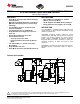
TERMINAL COMPONENTS (continued)
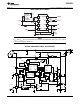
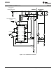
TERMINAL
I/O DESCRIPTION
(1) (2) (3)
NAME NO.
C
VDD
is the greater of:
or
(3)
VDD 6 I
where:
• I
DD
is the operating current of the UCC28600
(6)
• C
ISS
is the input capacitance of MOSFET M
1
• V
OUT(hi)
is VOH of the OUT pin, either 13 V (typ) V
OUT
clamp or less as measured
• f
QR(max)
is f
S
at high line, maximum load
(6)
• T
BURST
is the measured burst mode period
• ΔVDD
(burst)
is the allowed V
DD
ripple during burst mode
• ΔVDD
(uvlo)
is the UVLO hysteresis
(6)
• V
DS1(os)
is the amount of drain-source overshoot voltage
• L
LEAKAGE
is the leakage inductance of the primary winding
• C
D
is the total drain node capacitance of MOSFET M
1
• I
STARTUP
is I
DD
start-up current of the UCC28600
(6)
• C
SNUB
is the snubber capacitor value
• t
SS
is the soft start charge time
(7)
(6) Refer to the Electrical Characteristics Table for constant parameters.
(7) Refer to the UCC28600 Design Calculator (TI Literature Number SLVC104) or laboratory measurements for currents, voltages and times
in the operational circuit.
Copyright © 2005–2011, Texas Instruments Incorporated 9