Using the UCC28610EVM-474 User's Guide Literature Number: SLUU383C November 2009 – Revised June 2011
SLUU383C – November 2009 – Revised June 2011 Submit Documentation Feedback Copyright © 2009–2011, Texas Instruments Incorporated
User's Guide SLUU383C – November 2009 – Revised June 2011 UCC28610EVM-474 25-W Universal Off-Line Flyback Converter 1 Introduction The UCC28610EVM-474 evaluation module is a 25-W off-line Discontinuous Mode (DCM) flyback converter providing 12 V at 2.1-A maximum load current, operating from a universal AC input. The module is controlled with the UCC28610 Green-Mode Flyback Controller which uses a cascoded architecture that allows fully integrated current control without an external sense resistor.
Description 2.1 www.ti.com Applications The UCC28610 is suited for use in isolated off-line systems requiring high efficiency and advanced fault protection features including: • AC/DC Adaptors that have a Peak Power Output of 12 W to 65 W • Housekeeping and Auxiliary Power Supplies • Off-line Battery Chargers • Consumer Electronics (DVD players, set-top boxes, gaming, printers, etc.) 2.
Electrical Performance Specifications www.ti.com 3 Electrical Performance Specifications Table 1. UCC28610EVM-474 Electrical Performance Specifications PARAMETER CONDITIONS MIN NOM MAX UNITS INPUT CHARACTERISTICS VIN Input voltage IIN Input current VUVLO 85 Brown out 265 VRMS VIN = 115 VRMS, IOUT = max 0.3 A VIN = 115 VRMS, IOUT = 0 A 0.
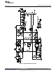
Schematic/Revision Code Placement 4 www.ti.com Schematic/Revision Code Placement NOTE: For revision A versions of the evaluation module, please refer to Appendix A of this user's guide for the schematic, list of materials and board layout. The EVM revision code can be found on the lower right corner of the top side of the board, as shown in Figure 1. TEXAS I NSTRUMENTS Figure 1. Placement of Revision Code for the Evaluation Module.
Schematic/Revision Code Placement + + + + www.ti.com Figure 2.
Schematic/Revision Code Placement 4.1 www.ti.com Circuit Description A brief description of the circuit elements follows: • Diode bridge D1, input capacitor C9, transformer (a.k.a. flyback inductor) T1, HV MOSFET Q1, UCC28610 controller U1, Schottky rectifier D6, Output capacitors C15 and C16 form the power stage of the converter. Note that the UCC28610 U1 is part of the power stage. This is because the DRV and GND pins carry the full peak primary side current of the converter.
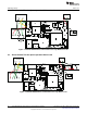
EVM Test Set Up www.ti.com 5 EVM Test Set Up Figure 2 shows the equipment set up when measuring the input power consumption during no load. Note the addition of the 10-Ω shunt resistor in Figure 3. During the no-load test, the power analyzer should be set for long averaging in order to include several cycles of operation and an appropriate current scale factor for using the external shunt must be used. Figure 3 shows the basic test set up recommended to evaluate the UCC28610EVM-474 with a load.
EVM Test Set Up 5.2 www.ti.com Recommended Test Set Up for Operation Without a Load DMM V 1 AC SOURCE Neutral + - Line TEXAS INSTRUMENTS POWER METER + - + V HI VLO AHI A LO Oscilloscope A EXT 10 Figure 3. UCC28610EVM-474 Recommended Test Set Up Without a Load 5.3 Recommended Test Set Up for Operation With a Load DMM V 1 AC SOURCE + Neutral - Line TEXAS I NSTRUMENTS DMM A 1 + - ELECTRONIC LOAD + - POWER METER + - + VHI VLO AHI ALO Oscilloscope AEXT Figure 4.
EVM Test Set Up www.ti.com 5.4 List of Test Points Table 2. Test Point Functional Description TEST POINT NAME DESCRIPTION +Vout Output voltage of EVM; this designator is not populated with a pin in order to facilitate tip and barrel output ripple voltage measurements. TP2 -Vout Return of the output of the EVM, secondary side GND reference.
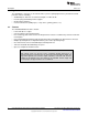
Test Procedure 6 www.ti.com Test Procedure All tests should use the set up as described in Section 5 of this user’s guide. The following test procedure is recommended primarily for power up and shutting down the evaluation module. Never leave a powered EVM unattended for any length of time. 6.1 Applying Power to the EVM 1. Set up the EVM as shown in Section 5 of this user’s guide (a) If no-load input power measurements are to be made, set the power analyzer to long averaging and external shunt mode.
Test Procedure www.ti.com 6.3 Output Voltage Regulation and Efficiency 1. For load regulation: (a) Use the test set up shown in Figure 4. (i) Be sure to remove the external shunt from the power analyzer and set the analyzer to normal mode (not long averaging). (b) Set the AC source to a constant voltage between 85 VAC and 265 VAC. (c) Apply power to the EVM per Section 6.1. (d) Vary the load current from 0 A up to 2.1 A, as measured on DMM A1.
Performance Data and Typical Characteristic Curves 7 www.ti.com Performance Data and Typical Characteristic Curves Figure 6 through Figure 23 present typical performance curves for the UCC28610EVM-474. EFFICIENCY vs. LOAD CURRENT 0.870 0.860 E F F IC IE N C Y 0.850 85VAC 0.840 115VAC 230VAC 0.830 264VAC 0.820 0.810 0.800 0.5 0.7 0.9 1.1 1.3 1.5 1.7 1.9 2.1 2.3 LOAD (A) Figure 6. Efficiency as a Function of Load Current and Input Voltage No-Load Power Consumption vs.
Performance Data and Typical Characteristic Curves www.ti.com FB CURRENT vs. DRV CURRENT 1800 1600 1400 ID R V ( m A ) 1200 85Vac 1000 115Vac 230Vac 800 265Vac 600 400 200 0 0 50 100 150 200 250 300 350 IFB (uA) Figure 8. DRV Current as a Function of FB Current FB CURRENT vs. SWITCHING FREQUENCY 140 120 F sw ( kH z ) 100 85Vac 80 115Vac 230Vac 60 265Vac 40 20 0 0 50 100 150 200 250 300 350 IFB (uA) Figure 9.
Performance Data and Typical Characteristic Curves www.ti.com OUTPUT VOLTAGEvs LOAD CURRENT O UTPUT VO LTAG E (V) 12.8 12.3 85Vac 115Vac 230Vac 11.8 265Vac 11.3 10.8 0 0.5 1 1.5 2 2.5 3 LOAD CURRENT (A) Figure 10. Output Voltage as a Function of Load Current and Line Voltage (Note the shutdown/retry threshold for each line voltage.) Figure 11. Start-Up Waveform (Input voltage = 115 VAC, full load. Ch.1 = bulk input voltage, 100 V/div., Ch.2 = VGG, 10 V/div., Ch.3 = VDD, 10V/div., Ch.
Performance Data and Typical Characteristic Curves www.ti.com Figure 12. FM Mode Switching Cycle Waveform (Input voltage = 115 VAC, full load, fSW = 112 kHz. Ch.1 = IDRV, 500 mA/div., IDRV = 1.53 A, Ch.2 = Drain of HV MOSFET, 100 V/div., Ch.3 = ZCD, 5 V/div.) Figure 13. AM Mode Switching Cycle Waveform (Input voltage = 85 VAC, 0.3-A load, fSW = 28.2 kHz, Ch.1 = IDRV, 500 mA/div., IDRV = 1.1 A, Ch.2 = Drain of HV MOSFET, 100 V/div., Ch.3 = ZCD, 5 V/div., Ch. 4 = VDD, 10 V/div.
Performance Data and Typical Characteristic Curves www.ti.com Figure 14. GM Mode Switching Cycle Waveform (Input voltage = 85 VAC, 0-A load, fSW = 28 kHz, Ch.1 = IDRV, 500 mA/div., IDRV = 440 mA, Ch.2 = Drain of HV MOSFET, 100 V/div., Ch.3 = ZCD, 5 V/div., Ch. 4 = VDD, 10 V/div.) Figure 15. Ripple on VGG and VDD During Green Mode Operation (Ch.3 = VGG, AC coupled, 2 V/div., Ch.4 = VDD, AC coupled, 200 mV/div.
Performance Data and Typical Characteristic Curves www.ti.com Figure 16. Output Voltage Ripple During Green Mode Operation (Input voltage = 85 VAC, no load. Ch.2 = VOUT, AC coupled, 20 mV/div.) Figure 17. Output Voltage Ripple During Frequency Modulation Mode (Input voltage = 85 VAC, full load. Ch.2 = VOUT, AC coupled, 20 mV/div.
Performance Data and Typical Characteristic Curves www.ti.com Figure 18. Load Transient, 0% to 100% Load Step (Ch.1 = IOUT, 2 A/div., Ch.2 = VOUT, AC coupled, 200 mV/div.) Figure 19. Brown-Out Protection (MOT shutdown/retry response triggered at full load when input voltage dropped to 72.4 VAC. Note the 750-ms tRETRY. Ch.1 = IDRV, Ch.3 = VDD, 10 V/div., Ch.4 = VGG, 10 V/div.
Performance Data and Typical Characteristic Curves www.ti.com Figure 20. Output Short Circuit Protection (Short circuit maintained on output; note the output current goes to 4.62 A, refer to equation 13 in the data sheet, during the 250-ms delay to overload fault, tOL, and retries after tRETRY = 750 ms. Input voltage = 85 VAC. Ch.1 = IOUT, 1 A/div., Ch. 3 = VOUT, 1 V/div.) Figure 21. Output Over Voltage Protection (The EVM was tested with an open FB loop, no load. OVP threshold is equal to 15.44 V. Ch.
Performance Data and Typical Characteristic Curves www.ti.com 60 180 40 120 20 60 0 0 -20 -60 -40 -120 -60 100 P h as e (de gr ees) G a i n (d B ) 115Vac Bode Plot -180 10000 1000 Frequency (Hz) Gain Phase Figure 22. Bode Plot (Input voltage = 115 VAC, full load.) 60 180 40 120 20 60 0 0 -20 -60 -40 -120 -60 100 P h as e (de gr ees) G a i n (d B ) 230Vac Bode Plot -180 10000 1000 Frequency (Hz) Gain Phase Figure 23. Bode Plot (Input voltage = 230 VAC, full load.
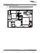
EVM Assembly Drawing and Layout www.ti.com 8 EVM Assembly Drawing and Layout Figure 24 through Figure 26 show the design of the UCC28610EVM-474 printed circuit board. TEXAS I NSTRUMENTS Figure 24.
EVM Assembly Drawing and Layout www.ti.com Figure 25. Bottom Layer Routing Figure 28. Bottom Layer Component Placement. Figure 26.
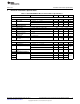
List of Materials www.ti.com 9 List of Materials Table 3. List of Materials for UCC28610EVM-474 COUNT REF DES DESCRIPTION PART NUMBER MFR 2 C1, C6 Capacitor, film, 0.33 µF, 275 VAC, X2, ±20%, 0.690 x 0.374 inch ECQ-U2A334ML Panasonic 1 C2 Capacitor, ceramic, 100 pF, 50 V, NP0, ±5%, 0603 Std Std C3 Capacitor, ceramic, not populated, 50 V, NP0, ±5%, 0603 Std Std 2 C4, C5 (optional) Capacitor, ceramic, 2200 pF, 250 VAC, X1/Y2, ±20%, 0.315 x 0.
References www.ti.com Table 3. List of Materials for UCC28610EVM-474 (continued) COUNT DESCRIPTION PART NUMBER MFR R1 Resistor, chip, 100 kΩ, 1/10 W, ±1%, 0603 Std Std 1 R2 Resistor, chip, 20.5 kΩ, 1/10 W, ±1%, 0603 Std Std 1 R3 Resistor, chip, 51.1 kΩ, 1/10 W, ±1%, 0603 Std Std 1 R4 Resistor, chip, 64.9 kΩ, 1/10 W, ±1%, 0603 Std Std 1 R5 Resistor, metal film, 169 kΩ, 1/2 W, ±1%, 0.300 x 0.100 inch SFR16S0001693FR500 Vishay/BC Components 1 R6 Resistor, chip, 68.
www.ti.com Appendix A A.1 UCC28610EVM-474 Rev. A + + + + The following schematic, board layout, and list of materials apply to the UCC28610EVM-474 Rev. A version of the evaluation module. The Rev. A version of the EVM includes differential mode inductors L2 and L3. Subsequent revisions of the EVM replaced these inductors with a short circuit. Figure 27. UCC28610EVM-474 Rev.
UCC28610EVM-474 Rev. A www.ti.com Figure 28. Top Side View of UCC28610EVM-474 Rev. A TEXAS I NSTRUMENTS Figure 29. Top Layer Component Placement for UCC28610EVM-474 Rev.
UCC28610EVM-474 Rev. A www.ti.com Figure 30. Bottom Layer Routing of UCC28610EVM-474 Rev. A Figure 31. Bottom Layer Component Placement of UCC28610EVM-474 Rev.
UCC28610EVM-474 Rev. A www.ti.com Table 4. Table 4. List of Materials for UCC28610EVM-474 Rev. A COUNT 30 REF DES DESCRIPTION PART NUMBER MFR 2 C1, C6 Capacitor, film, 0.33 µF, 275VAC, X2, ±20%, 0.690 x 0.374 inch ECQ-U2A334ML Panasonic 1 C2 Capacitor, ceramic, 100 pF, 50 V, NP0, ±5%, 0603 Std Std 0 C3 Capacitor, ceramic, not populated, 50 V, NP0, ±5%, 0603 Std Std 2 C4, C5 (optional) Capacitor, ceramic, 2200 pF, 250 VAC, X1/Y2, ±20%, 0.315 x 0.
UCC28610EVM-474 Rev. A www.ti.com Table 4. Table 4. List of Materials for UCC28610EVM-474 Rev. A (continued) COUNT REF DES DESCRIPTION PART NUMBER MFR 1 R1 Resistor, chip, 100 kΩ, 1/10 W, ±1%, 0603 Std Std 1 R2 Resistor, chip, 20.5 kΩ, 1/10 W, ±1%, 0603 Std Std 1 R3 Resistor, chip, 51.1 kΩ, 1/10 W, ±1%, 0603 Std Std 1 R4 Resistor, chip, 64.9 kΩ, 1/10 W, ±1%, 0603 Std Std 1 R5 Resistor, metal film, 169 kΩ, 1/2 W, ±1%, 0.300 x 0.
UCC28610EVM-474 Rev. A www.ti.com EVALUATION BOARD/KIT IMPORTANT NOTICE Texas Instruments (TI) provides the enclosed product(s) under the following conditions: This evaluation board/kit is intended for use for ENGINEERING DEVELOPMENT, DEMONSTRATION, OR EVALUATION PURPOSES ONLY and is not considered by TI to be a finished end-product fit for general consumer use. Persons handling the product(s) must have electronics training and observe good engineering practice standards.
IMPORTANT NOTICE Texas Instruments Incorporated and its subsidiaries (TI) reserve the right to make corrections, modifications, enhancements, improvements, and other changes to its products and services at any time and to discontinue any product or service without notice. Customers should obtain the latest relevant information before placing orders and should verify that such information is current and complete.