UCC28610 www.ti.
UCC28610 SLUS888F – JANUARY 2009 – REVISED SEPTEMBER 2012 www.ti.com This integrated circuit can be damaged by ESD. Texas Instruments recommends that all integrated circuits be handled with appropriate precautions. Failure to observe proper handling and installation procedures can cause damage. ESD damage can range from subtle performance degradation to complete device failure.
UCC28610 www.ti.com SLUS888F – JANUARY 2009 – REVISED SEPTEMBER 2012 ABSOLUTE MAXIMUM RATINGS (1) All voltages are with respect to GND, –40°C < TJ = TA < 125°C, all currents are positive into and negative out of the specified terminal (unless otherwise noted) UCC28610 VDD –0.5 to +25 DRV, during conduction –0.5 to +2.0 DRV, during non-conduction 20 VGG (2) Input voltage range ZCD, MOT, CL –0.5 to +16 (3) –0.5 to +1.
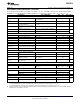
UCC28610 SLUS888F – JANUARY 2009 – REVISED SEPTEMBER 2012 www.ti.com ELECTRICAL CHARACTERISTICS Unless otherwise stated: VDD = 12 V, VGG = 12 V, ZCD = 1 V, IFB = 10 µA, GND = 0 V, a 0.1-μF capacitor between VDD and GND, a 0.1-μF capacitor between VGG and GND, RCL = 33.2 kΩ, RMOT = 380 kΩ, –40°C < TA < +125°C, TJ = TA PARAMETER TEST CONDITIONS MIN TYP MAX UNITS VDD and VGG SUPPLY VGG(OPERATING) VGG voltage, operating VDD = 14 V, IVGG = 2.
UCC28610 www.ti.com SLUS888F – JANUARY 2009 – REVISED SEPTEMBER 2012 ELECTRICAL CHARACTERISTICS (continued) Unless otherwise stated: VDD = 12 V, VGG = 12 V, ZCD = 1 V, IFB = 10 µA, GND = 0 V, a 0.1-μF capacitor between VDD and GND, a 0.1-μF capacitor between VGG and GND, RCL = 33.2 kΩ, RMOT = 380 kΩ, –40°C < TA < +125°C, TJ = TA PARAMETER TEST CONDITIONS MIN TYP MAX UNITS 5 20 50 mV -220 -160 -100 mV 0.1 0.15 0.
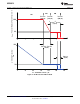
UCC28610 IDRV,PK - Percent of Maximum Peak DRV Current - % SLUS888F – JANUARY 2009 – REVISED SEPTEMBER 2012 www.ti.com AM FM IFB,CNR1 (165mA) 100 GM I FB,CNR2 (210mA) IFB,CNR3 (280mA) IFB,CNR3 - IFB,CNR2 (70mA) 33 133 IFB,CNR2 - IFB,CNR1 fS - Switching Frequency kHz (45mA) IGM,HYST (25mA) 30 0 50 100 150 200 250 300 I FB - Feedback Current - μA Figure 2.
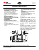
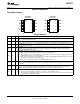
UCC28610 www.ti.com SLUS888F – JANUARY 2009 – REVISED SEPTEMBER 2012 DEVICE INFORMATION PIN CONFIGURATION D PACKAGE (Top View) P PACKAGE (Top View) FB 1 8 VDD FB 1 8 VDD ZCD 2 7 GND ZCD 2 7 GND CL 3 6 DRV CL 3 6 DRV MOT 4 5 VGG MOT 4 5 VGG PIN DESCRIPTIONS NAME PIN I/O DESCRIPTION CL 3 I (Current Limit) This pin programs the peak primary inductor current that is reached each switching cycle. Program with a resistor between CL and GND.
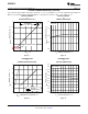
UCC28610 SLUS888F – JANUARY 2009 – REVISED SEPTEMBER 2012 www.ti.com TYPICAL CHARACTERISTICS Unless otherwise stated: VDD = 12V, VGG = 12V, ZCD = 1 V, IFB = 10 µA, GND = 0 V, a 0.1-μF capacitor between VDD and GND, a 0.1-μF capacitor between VGG and GND, RCL = 33.2 kΩ, RMOT = 380 kΩ, –40°C < TA < +125°C, TJ = TA BIAS SUPPLY CURRENT vs BIAS SUPPLY VOLTAGE DURING OPERATION BIAS SUPPLY CURRENT vs BIAS SUPPLY VOLTAGE DURING GREEN MODE 4.
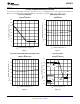
UCC28610 www.ti.com SLUS888F – JANUARY 2009 – REVISED SEPTEMBER 2012 TYPICAL CHARACTERISTICS (continued) Unless otherwise stated: VDD = 12V, VGG = 12V, ZCD = 1 V, IFB = 10 µA, GND = 0 V, a 0.1-μF capacitor between VDD and GND, a 0.1-μF capacitor between VGG and GND, RCL = 33.2 kΩ, RMOT = 380 kΩ, –40°C < TA < +125°C, TJ = TA OSCILLATOR FREQUENCY vs FEEDBACK CURRENT MINIMUM SWITCHING PERIOD vs TEMPERATURE 8.
UCC28610 SLUS888F – JANUARY 2009 – REVISED SEPTEMBER 2012 www.ti.com TYPICAL CHARACTERISTICS (continued) Unless otherwise stated: VDD = 12V, VGG = 12V, ZCD = 1 V, IFB = 10 µA, GND = 0 V, a 0.1-μF capacitor between VDD and GND, a 0.1-μF capacitor between VGG and GND, RCL = 33.2 kΩ, RMOT = 380 kΩ, –40°C < TA < +125°C, TJ = TA PEAK DRV CURRENT vs TRANSCONDUCTANCE (1/RCL) PEAK DRV CURRENT vs AMBIENT TEMPERATURE 3.
UCC28610 www.ti.com SLUS888F – JANUARY 2009 – REVISED SEPTEMBER 2012 TYPICAL CHARACTERISTICS (continued) Unless otherwise stated: VDD = 12V, VGG = 12V, ZCD = 1 V, IFB = 10 µA, GND = 0 V, a 0.1-μF capacitor between VDD and GND, a 0.1-μF capacitor between VGG and GND, RCL = 33.
UCC28610 SLUS888F – JANUARY 2009 – REVISED SEPTEMBER 2012 www.ti.com Block Diagram Fault Latch Reset 13V + VGG LDO Reg VDD Switch + 5 10V/6V VDD VGG Shunt 8 14V HS Drive UVLO + VGG 2V 10V/8V Enable PWM IFB FB 1 IFB IFB Feedback Processing 0?A < IFB < 210?A IFB > 210?A ZCD Green -mode IFB Enable PWM Overload D Zero Current Detect 2 Q V GATE Driver R 7.5k? Bulk Discharge OV Fault Output Voltage Sense DRV 1/t S Modulators IFB = 0 6 Freq.
UCC28610 www.ti.com SLUS888F – JANUARY 2009 – REVISED SEPTEMBER 2012 APPLICATION INFORMATION General Operation The flyback converter is attractive for low power AC/DC applications because it provides output isolation and wide input operating abilities using a minimum number of components. Operation of the flyback converter in Discontinuous Conduction Mode (DCM) is especially attractive because it eliminates reverse recovery losses in the output rectifier and it simplifies control.
UCC28610 SLUS888F – JANUARY 2009 – REVISED SEPTEMBER 2012 www.ti.com Transformer Selection To begin a power supply design, the power supply designer needs to know the peak power to be delivered by the converter, the input voltage range, the output voltage, and an estimate of the maximum allowable bulk voltage ripple. Select the maximum allowable stress voltage for the external power MOSFET.
UCC28610 www.ti.com SLUS888F – JANUARY 2009 – REVISED SEPTEMBER 2012 Assume a deadtime, tDT, of 5% of the total minimum switching period to allow for variations in the output capacitance of the HVMOSFET and the leakage inductance value: tDT = 0.
UCC28610 SLUS888F – JANUARY 2009 – REVISED SEPTEMBER 2012 www.ti.com Cascode Bias and Start-Up The UCC28610 uses a cascode drive and bias to control the high voltage power MOSFET and provide initial bias at start-up. Thus, the external high voltage power MOSFET provides the start-up function in addition to the power switching function during converter operation.
UCC28610 www.ti.com SLUS888F – JANUARY 2009 – REVISED SEPTEMBER 2012 The UCC28610 integrates the low voltage switch in the form of a 90-mΩ FET along with all associated current sensing and drive. The HVMOSFET is forced to track the fast internal low voltage driver. The drain-gate charge in the HVMOSFET does not affect the turn-off speed because the gate is connected to a low impedance DC source.
UCC28610 SLUS888F – JANUARY 2009 – REVISED SEPTEMBER 2012 www.ti.com In order to achieve the lowest possible no-load power, select the number of turns in the bias winding so that VDD is higher than 16 V – VTH of the HVMOSFET. A bias winding voltage between 17 V and 20 V usually achieves minimum loss. The bias winding often tracks the primary leakage inductance turn-off voltage spike. Place a 20-V Zener diode between VDD and GND in applications where heavy loads cause excessive VDD voltage.
UCC28610 www.ti.com SLUS888F – JANUARY 2009 – REVISED SEPTEMBER 2012 Feedback Function Modulation and modes are controlled by applying current to the FB pin. The FB pin is usually used to feed back the output error signal to the modulator. The UCC28610 uses internal current mirrors to apply the FB current to the Feedback Processing block, and then to the Frequency Modulator and Current Modulator blocks. The voltage of the FB pin is a constant 0.7 V.
UCC28610 SLUS888F – JANUARY 2009 – REVISED SEPTEMBER 2012 www.ti.com Modulation Modes Under normal operating conditions, the FB current commands the operating mode of the UCC28610, as shown in Figure 25 and Figure 26. The FB current commands the UCC28610 to operate the converter in one of three modes: Frequency Modulation (FM) mode, Amplitude Modulation (AM) mode, and Green Mode (GM). The converter operates in FM mode with a large power load (22% to 100% the peak regulated power).
UCC28610 www.ti.com SLUS888F – JANUARY 2009 – REVISED SEPTEMBER 2012 Primary Current Sense The UCC28610 uses a current mirror technique to sense primary current in the Current Modulator. See Figure 27 for details. All of the primary current passes into the DRV pin, through the Driver MOSFET and out of the GND pin. The Driver MOSFET current is scaled and reflected to the PWM Comparator where it is compared with the CL current.
UCC28610 SLUS888F – JANUARY 2009 – REVISED SEPTEMBER 2012 www.ti.com Zero Crossing Detection The modulator requires three conditions in order to initiate the next switching cycle: 1. The time since the last turn-on edge must be equal to or greater than the time that is requested by the Feedback Processor as determined by the feedback current, IFB. 2. The time since the last turn-on edge must be longer than the minimum period that is built into the UCC28610 (nominally 7.5 μs which equals 133 kHz). 3.
UCC28610 www.ti.com SLUS888F – JANUARY 2009 – REVISED SEPTEMBER 2012 Zero crossing is detected using a resistive divider across the bias winding, as shown in Figure 29. The bias winding operates in phase with the output winding. The ZCD function detects transformer demagnetization when the ZCD voltage has a high to low crossing of the 20-mV ZCD threshold, ZCDTH. The voltage at the ZCD pin is internally clamped to contain negative excursions at -160mV (ZCDCLAMP).
UCC28610 SLUS888F – JANUARY 2009 – REVISED SEPTEMBER 2012 www.ti.com Green Mode Operation During light load operation the UCC28610 cycles between two states: GM-on and GM-off. The details are shown in Figure 30. During the GM-on state, the controller is active while the modulator issues a burst of one or more pulses. During the GM-off state the controller reduces its operating current and switching action is inhibited.
UCC28610 www.ti.com SLUS888F – JANUARY 2009 – REVISED SEPTEMBER 2012 Maximum Converter Power Limitation The suggested peak power range of the UCC28610 is 12 W to 65 W based on a universal AC line converter (90VAC to 265-VAC input line voltage), using an external high voltage MOSFET with a voltage rating of 600 V. This power range may depend on application and external MOSFET stress voltage. Ultimately, the peak primary current is the limiting factor because this current must pass through the UCC28610.
UCC28610 SLUS888F – JANUARY 2009 – REVISED SEPTEMBER 2012 www.ti.com Fault Recovery The UCC28610 reacts with the programmed overload response if the overload lasts longer than tOL (nominally 250 ms). The overload fault responses are either (1) latch-off or (2) shutdown/retry after a retry delay of 750 ms. The overload response is programmed with the MOT pin. The forced DCM feature prevents transformer saturation and limits the average and RMS output currents of the secondary winding of the transformer.
UCC28610 www.ti.com SLUS888F – JANUARY 2009 – REVISED SEPTEMBER 2012 Maximum On-Time and Brown Out The forced DCM feature provides protection against excessive primary currents in the event that the input voltage becomes very low. The highest possible secondary currents can be described by Equation 16. The UCC28610 adds further protection by allowing the user to program the maximum on-time.
UCC28610 SLUS888F – JANUARY 2009 – REVISED SEPTEMBER 2012 www.ti.com Over Voltage Detection The UCC28610 controller monitors the output voltage by sampling the voltage at the auxiliary winding. The sampling time has a fixed delay of 1 μs, tBLANK,OVP, after the internal driver turns off. This allows the auxiliary winding to be sampled after the bias winding voltage settles from the transient.
UCC28610 www.ti.com SLUS888F – JANUARY 2009 – REVISED SEPTEMBER 2012 Avoid HF Ringing High frequency ringing problems with cascode MOSFET drives can often be avoided. Many converters will not have this problem because they use an HVMOSFET with a large Vth, large RDS(on), low transconductance gain, or operate at low current. Ringing problems can also be avoided by minimizing stray inductance. The trace between the HVMOSFET source and the DRV pin must be kept very short, less than 1 cm.
UCC28610 SLUS888F – JANUARY 2009 – REVISED SEPTEMBER 2012 www.ti.com Ferrite Chip or Bead Solution The ferrite chip or bead connected to the gate of the HVMOSFET provides the best result because it suppresses ringing in the gate, source, and drain circuits of the HVMOSFET with minimal added losses. Select the ferrite chip for its resistance value in the ringing frequency range (for example, 60 Ω at 100 MHz).
UCC28610 www.ti.com SLUS888F – JANUARY 2009 – REVISED SEPTEMBER 2012 Typical Schematic and Layout It is possible to design a power supply on a single layer board using the UCC28610. Figure 36 and Figure 37 show an example of a typical layout and design, respectively. Proper use of ground planes can solve EMI and thermal problems. For best results, create a quiet ground plane for the components associated with pins 1 through 4. This offers shielding for the control signals.
UCC28610 www.ti.com + + + + SLUS888F – JANUARY 2009 – REVISED SEPTEMBER 2012 Figure 37.
UCC28610 www.ti.com SLUS888F – JANUARY 2009 – REVISED SEPTEMBER 2012 Terminal Components For reference designators refer to Figure 1. Table 1. Terminal Components NAME TERMINAL DESCRIPTION R CL = 33.2k W ´ CL IDRV(PK) = 3 K P ´ LM PIN 100 kV RCL Where KP = 0.54W/ μH LM is the minimum value of the primary inductance PIN = POUT/η η = efficiency Q1, power MOSFET with adequate voltage and current ratings, VVGS must have at least 20-V static rating.
UCC28610 SLUS888F – JANUARY 2009 – REVISED SEPTEMBER 2012 www.ti.com Table 1.
UCC28610 www.ti.com SLUS888F – JANUARY 2009 – REVISED SEPTEMBER 2012 Changes from Revision E (July, 2011) to Revision F Page • Changed updated typical application drawing on first page. ................................................................................................ 1 • Changed Recommended Operating Conditions Application drawing. .................................................................................. 2 • Changed ESD Rating, Human Body Model from 2.0 kV to 1.5 kV. .......
PACKAGE MATERIALS INFORMATION www.ti.com 17-Aug-2012 TAPE AND REEL INFORMATION *All dimensions are nominal Device UCC28610DR Package Package Pins Type Drawing SOIC D 8 SPQ Reel Reel A0 Diameter Width (mm) (mm) W1 (mm) 2500 330.0 12.4 Pack Materials-Page 1 6.4 B0 (mm) K0 (mm) P1 (mm) 5.2 2.1 8.0 W Pin1 (mm) Quadrant 12.
PACKAGE MATERIALS INFORMATION www.ti.com 17-Aug-2012 *All dimensions are nominal Device Package Type Package Drawing Pins SPQ Length (mm) Width (mm) Height (mm) UCC28610DR SOIC D 8 2500 340.5 338.1 20.
IMPORTANT NOTICE Texas Instruments Incorporated and its subsidiaries (TI) reserve the right to make corrections, enhancements, improvements and other changes to its semiconductor products and services per JESD46, latest issue, and to discontinue any product or service per JESD48, latest issue. Buyers should obtain the latest relevant information before placing orders and should verify that such information is current and complete.