
Datasheet


Off-line Power Supply Controller
• Transformerless Off-line
Applications
• Ideal Primary-side Bias Supply
• Efficient BiCMOS Design
• Wide Input Range
• Fixed or Adjustable
Low Voltage Output
• Uses Low Cost SMD Inductors
• Short Circuit Protected
• Optional Isolation Capability
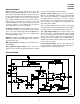
The UCC1889 controller is optimized for use as an off-line, low power, low voltage,
regulated bias supply. The unique circuit topology utilized in this device can be
visualized as two cascaded flyback converters, each operating in the discontinu-
ous mode, and both driven from a single external power switch. The significant
benefit of this approach is the ability to achieve voltage conversion ratios of 400V
to 12V with no transformer and low internal losses.
The control algorithm utilized by the UCC1889 is to force the switch on time to be
inversely proportional to the input line voltage while the switch off time is made in-
versely proportional to the output voltage. This action is automatically controlled by
an internal feedback loop and reference. The cascaded configuration allows a volt-
age conversion from 400V to 12V to be achieved with a switch duty cycle greater
than 10%. This topology also offers inherent short circuit protection since as the
output voltage falls to zero, the switch off time approaches infinity.
The output voltage can be easily set to 12V or 18V. Moreover, it can be pro-
grammed for other output voltages less than 18V with a few additional compo-
nents. An isolated version can be achieved with this topology as described further
in Unitrode Application Note U-149.
UCC1889
UCC2889
UCC3889
SLUS158A - FEBRUARY 1995 - REVISED FEBRUARY 2003
FEATURES
DESCRIPTION
OPERATION
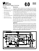
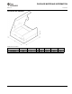
With reference to the application diagram below, when input voltage is first applied,
the RON current into TON is directed to VCC where it charges the external capacitor,
C3, connected to VCC. As voltage builds on VCC, an internal undervoltage lockout
holds the circuit off and the output at DRIVE low until VCC reaches 8.4V. At this
time, DRIVE goes high turning on the power switch, Q1, and redirecting the current
into TON to the timing capacitor, CT. CT charges to a fixed threshold with a current
ICHG=0.8 • (VIN - 4.5V)/RON. Since DRIVE will only be high for as long as CT
charges, the power switch on time will be inversely proportional to line voltage.
This provides a constant line voltage-switch on time product.
Note: This device incorporates patented technology used under license from Lambda Electronics, Inc.
TYPICAL APPLICATION
UDG-93060-1