
Datasheet

SLUS542F − OCTOBER 2003 − REVISED JULY 2009
1
www.ti.com
FEATURES
D
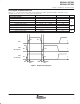
Low Output Jitter
D Soft−Stop Shutdown of MAIN and AUX
D Ideal for Active Clamp/Reset Forward,
Flyback Converters
D Provides Complementary Auxiliary Driver
with Programmable Deadtime (Turn-On
Delay) between AUX and MAIN Switches
D Peak Current-Mode Control with
Cycle-by-Cycle Current Limiting
D 110-V Input Startup Regulator on UCC2891/3
D TrueDrivet 2-A Sink, 2-A Source Outputs
D Accurate Line UV and Line OV Threshold
D Programmable Slope Compensation
D 1.0-MHz Synchronizable Oscillator
D Precise Programmable Maximum Duty Cycle
D Programmable Soft Start
APPLICATIONS
D
150-W to 700-W SMPS
D High-Efficiency, Low EMI/RFI Off-Line or
DC/DC Converters
D Server, 48-V Telecom, Datacom
D High Power Adapter, LCD-TV and PDP-TV
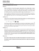
DESCRIPTION
The UCC2891/2/3/4 family of PWM controllers is
designed to simplify implementation of the various
active clamp/reset switching power topologies.
The UCC289x is a peak current-mode, fixed-
frequency, high-performance pulse width modulator.
It includes the logic and the drive capability for the
auxiliary switch with a simple method of
programming the critical delays for proper active
clamp operation.
The UCC2891/3 includes a 110-V start-up
regulator for initial start-up and to provide
keep-alive power during stand-by.
Additional features include an internal
programmable slope compensation circuit,
precise D
MAX
limit, and a single resistor
programmable synchronizable oscillator. An
accurate line monitoring function also programs
the converter’s ON and OFF transitions with
regard to the bulk input voltage. Along with the
UCC2897, this UCC289x family allows the power
supply designer to eliminate many of the external
components, reducing the size and complexity of
the design.
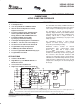
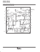
5
13
12
16
15
1
2
3
RDEL
RTON
RTOFF
SYNC
LINE UV
OUT
AUX
PGND
4 VREF
11
VIN
UCC2891
6 GND
7CS
8 RSLOPE
14VDD
SS/SD
10
FB
9
SECONDARY
SIDE E/A
Q1
Q2
LOAD
SR
DRIVE
BIAS
WINDING
+VIN
D3
Q3
D4
Q4
Lo
Co
D2
D1
R
DEL
R
ON
R
OFF
R
SLOPE
R
F
C
F
C
VREF
C
BIAS
C
SS
C
AUX
C
CLAMP
C
BULK
R
OUT
R
CS
D
AUX
! " #$%! " &$'(#! )!%*
)$#!" # ! "&%##!" &% !+% !%" %," "!$%!"
"!)) -!.* )$#! &#%""/ )%" ! %#%""(. #($)%
!%"!/ (( &%!%"*
Copyright 2003 − 2009, Texas Instruments Incorporated
Please be aware that an important notice concerning availability, standard warranty, and use in critical applications of
Texas Instruments semiconductor products and disclaimers thereto appears at the end of this data sheet.