
Datasheet


UCC2897A
SLUS829D -- AUGUST 2008 -- REVISED JULY 2009
ADVANCED CURRENT-MODE
ACTIVE CLAMP PWM CONTROLLER
1
www.ti.com
FEATURES
D Low Output Jitter
D “Soft Stop” shut down of MAIN and AUX
D 110-V Input Startup Function
D Ideal for Active Clamp/Reset Forward,
Flyback and Synchronous Rectifier Uses
D Provides Complementary Auxiliary Driver
with Programmable Deadtime (Turn-On
Delay) between AUX and MAIN Switches
D Peak Current-Mode Control with 0.5-V
Cycle-by-Cycle Current Limiting
D TrueDrivet 2-A Sink, 2-A Source Outputs
D Trimmed Internal Bandgap Reference for
Accurate Line UV and Line OV Threshold
D Programmable Slope Compensation
D High-Performance 1.0-MHz Synchronizable
Oscillator with Internal Timing Capacitor
D Precise Programmable Maximum Duty Cycle
D PB-Free Lead Finish Package
APPLICATIONS
D High-Efficiency DC/DC Power Supplies
D Server Power, 48-V Telecom, Datacom, and
42-V Automotive Applications
DESCRIPTION
The UCC2897A PWM controller simplifies
implementation of the various active clamp/reset
and synchronous rectifier switching power
topologies.
The UCC2897A is a peak current-mode, fixed-
frequency, high-performance pulse width modulator .
It includes the logic and the drive capability for the
P-channel auxiliary switch along with a simple
method of programming the critical delays for
proper active clamp operation.
Features include an internal programmable slope
compensation circuit, precise D
MAX
limit, and a
synchronizable oscillator with an internal timing
capacitor. An accurate line monitoring function
also programs the converter’s ON and OFF
transitions with regard to the bulk input voltage,
VIN.
The UCC2897A adds a second level hiccup mode
current sense threshold, bi-directional
synchronization and input overvoltage protection
functionalities. The UCC2897A is offered in 20-pin
TSSOP (PW) and 20-pin QFN (RGP) package.
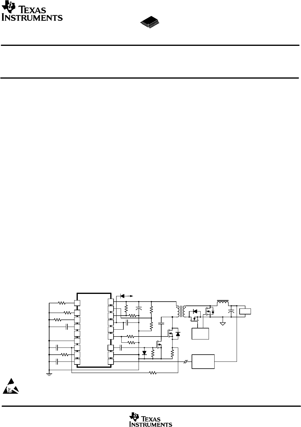
TYPICAL APPLICATION DIAGRAM
C
BIAS
R
OUT
C
AUX
D
AUX
L
O
7
15
14
1
18
3
4
5
RDEL
RON
ROFF
SYNC
LINEUV
OUT
AUX
PGND
6VREF
13
R
DEL
LINEOV
UCC2897A
8GND
9CS
10 RSLOPE
17VDD
FB
11
C
VREF
R
ON
R
OFF
R
SLOPE
C
F
SECONDARY
SIDE E/A
Q1
Q2
C
O
LOAD
SR
DRIVE
BIAS
WINDING
+VIN
19
16
VIN
PVDD
SS/SD12
C
SS
D1
D3
Q3
D4
Q4
These devices have limited built -in ESD protection. The leads should be shorted together or the device placed in conductive foam
during storage or handling to prevent electrostatic damage to the MOS gates.
PRODUCTION DATA information is curre nt as of publication date.
Products conform to specifications per the terms of Texas Instruments
standard warranty. Production processing does not necessarily include
testing of all parameters.
Copyright © 2008 -- 2009, Texas Instruments Incorporated