UCC28C40, UCC28C41, UCC28C42, UCC28C43, UCC28C44, UCC28C45 UCC38C40, UCC38C41, UCC38C42, UCC38C43, UCC38C44, UCC38C45 SLUS458E -- AUGUST 2001 -- REVISED OCTOBER 2010 BiCMOS LOW-POWER CURRENT-MODE PWM CONTROLLER FEATURES DESCRIPTION D Enhanced Replacement for UC3842A Family D D D D D D D D D D UCC38C4x family is a high-performance currentmode PWM controller. It is an enhanced BiCMOS version with pin-for-pin compatibility to the industry standard UC384xA family and UC384x family of PWM controllers.
UCC28C40, UCC28C41, UCC28C42, UCC28C43, UCC28C44, UCC28C45 UCC38C40, UCC38C41, UCC38C42, UCC38C43, UCC38C44, UCC38C45 SLUS458E -- AUGUST 2001 -- REVISED OCTOBER 2010 recommended operating conditions MIN MAX Input voltage, VDD 18 Output voltage range, VOUT 18 V 200 mA --20 mA 105 °C Average output current, IOUTW Reference output current, IOUT(ref)W Operating junction temperature, TJW ¶ UNIT --40 V It is not recommended that the device operate under conditions beyond those specified in this
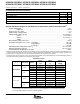
UCC28C40, UCC28C41, UCC28C42, UCC28C43, UCC28C44, UCC28C45 UCC38C40, UCC38C41, UCC38C42, UCC38C43, UCC38C44, UCC38C45 SLUS458E -- AUGUST 2001 -- REVISED OCTOBER 2010 electrical characteristics VDD = 15 V (See Note 1), RT = 10 kΩ, CT = 3.3 nF, CVDD = 0.
UCC28C40, UCC28C41, UCC28C42, UCC28C43, UCC28C44, UCC28C45 UCC38C40, UCC38C41, UCC38C42, UCC38C43, UCC38C44, UCC38C45 SLUS458E -- AUGUST 2001 -- REVISED OCTOBER 2010 electrical characteristics VDD = 15 V (See Note 1), RT = 10 kΩ, CT = 3.3 nF, CVDD = 0.1μF and no load on the outputs, TA = --40°C to 105°C for the UCC28C4x and TA = 0°C to 70°C for the UCC38C4x, TA = TJ (unless otherwise noted) PARAMETER TEST CONDITIONS MIN TYP MAX UNITS Output Section VOUT low (RDS(on) pull-down) ISINK = 200 mA 5.
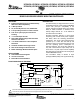
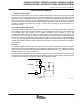
UCC28C40, UCC28C41, UCC28C42, UCC28C43, UCC28C44, UCC28C45 UCC38C40, UCC38C41, UCC38C42, UCC38C43, UCC38C44, UCC38C45 SLUS458E -- AUGUST 2001 -- REVISED OCTOBER 2010 pin assignments COMP: This pin provides the output of the error amplifier for compensation. In addition, the COMP pin is frequently used as a control port by utilizing a secondary-side error amplifier to send an error signal across the secondary-primary isolation boundary through an opto-isolator.
UCC28C40, UCC28C41, UCC28C42, UCC28C43, UCC28C44, UCC28C45 UCC38C40, UCC38C41, UCC38C42, UCC38C43, UCC38C44, UCC38C45 SLUS458E -- AUGUST 2001 -- REVISED OCTOBER 2010 APPLICATION INFORMATION This device is a pin-for-pin replacement of the bipolar UC3842 family of controllers, the industry standard PWM controller for single-ended converters. Familiarity with this controller family is assumed.
UCC28C40, UCC28C41, UCC28C42, UCC28C43, UCC28C44, UCC28C45 UCC38C40, UCC38C41, UCC38C42, UCC38C43, UCC38C44, UCC38C45 SLUS458E -- AUGUST 2001 -- REVISED OCTOBER 2010 APPLICATION INFORMATION ± 1% initial reference voltage The BiCMOS internal reference of 2.5 V has an enhanced design and utilizes production trim to allow initial accuracy of ±1% at room temperature and ± 2% over the full temperature range.
UCC28C40, UCC28C41, UCC28C42, UCC28C43, UCC28C44, UCC28C45 UCC38C40, UCC38C41, UCC38C42, UCC38C43, UCC38C44, UCC38C45 SLUS458E -- AUGUST 2001 -- REVISED OCTOBER 2010 APPLICATION INFORMATION oscillator synchronization The UCC38C4x oscillator has the same synchronization characteristics as the original bipolar devices. Thus, the information in the Application Note U--100A, UC3842/3/4/5 Provides Low-Cost Current-Mode Control, (TI Literature No. SLUA143) still applies.
UCC28C40, UCC28C41, UCC28C42, UCC28C43, UCC28C44, UCC28C45 UCC38C40, UCC38C41, UCC38C42, UCC38C43, UCC38C44, UCC38C45 SLUS458E -- AUGUST 2001 -- REVISED OCTOBER 2010 APPLICATION INFORMATION precautions The absolute maximum supply voltage is 20 V, including any transients that may be present. If this voltage is exceeded, device damage is likely. This is in contrast to the predecessor bipolar devices, which could survive up to 30 V.
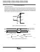
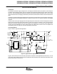
www.ti.com 46.4k 0.1uF C5 7 6 5 4 3 2 AGnd Ref Rt FB SS SD OVS R12 200 ucc3961 U1 R2 2 1 C7 8 9 10 11 12 13 14 T2 100pF Vs CS PGnd Out Vdd St UVS 2.4k R3 1.2k 4 3 R4 1.5k 300 R13 C8 1uF Q2 470pF C6 76.8k R5 R6 4.7 C25 0.047uF C10 2.7nF 0.1uF C9 R8 R10 1k 5.1k D1 R14 50k R15 20k 40% 0.33 R9 Q1 C22 4.7nF 20k R24 20k 402 R23 Q3 R25 20k 680pF 100 R28 R19 20 4.7 R26 C17 4700pF 3300pF C12 5.6nF C16 21.
UCC28C40, UCC28C41, UCC28C42, UCC28C43, UCC28C44, UCC28C45 UCC38C40, UCC38C41, UCC38C42, UCC38C43, UCC38C44, UCC38C45 SLUS458E -- AUGUST 2001 -- REVISED OCTOBER 2010 TYPICAL CHARACTERISTICS OSCILLATOR FREQUENCY vs TIMING RESISTANCE AND CAPACITANCE OSCILLATOR DISCHARGE CURRENT vs TEMPERATURE 9.5 10 M CT = 470 pF 1M f -- Frequency -- Hz IDISCH -- Oscillator Discharge Current -- mA CT = 220 pF CT = 1 nF 100 k 10 k CT = 4.7 nF CT = 2.2 nF 1k 1k 10 k 9.0 8.5 8.0 7.5 7.
UCC28C40, UCC28C41, UCC28C42, UCC28C43, UCC28C44, UCC28C45 UCC38C40, UCC38C41, UCC38C42, UCC38C43, UCC38C44, UCC38C45 SLUS458E -- AUGUST 2001 -- REVISED OCTOBER 2010 TYPICAL CHARACTERISTICS REFERENCE VOLTAGE vs TEMPERATURE ERROR AMPLIFIER REFERENCE VOLTAGE vs TEMPERATURE 2.55 VEAREF -- Error Amplifier Reference Voltage -- V 5.05 VREF -- Reference Voltage -- V 5.04 5.03 5.02 5.01 5.00 4.99 4.98 4.97 4.96 4.95 --50 --25 0 25 50 75 100 2.54 2.53 2.52 2.51 2.50 2.49 2.48 2.47 2.46 2.
UCC28C40, UCC28C41, UCC28C42, UCC28C43, UCC28C44, UCC28C45 UCC38C40, UCC38C41, UCC38C42, UCC38C43, UCC38C44, UCC38C45 SLUS458E -- AUGUST 2001 -- REVISED OCTOBER 2010 TYPICAL CHARACTERISTICS 16 UNDERVOLTAGE LOCKOUT vs TEMPERATURE (UCC38C43 & UCC38C45) UNDERVOLTAGE LOCKOUT vs TEMPERATURE (UCC38C42 & UCC38C44) 9.0 15 VUVLO -- UVLO Voltage -- V 13 UVLO ON 12 UVLO OFF 11 10 9 8.6 8.4 8.2 8.0 7.8 7.6 8 7.4 7 7.2 --50 --25 0 25 50 75 100 125 UVLO OFF 7.
UCC28C40, UCC28C41, UCC28C42, UCC28C43, UCC28C44, UCC28C45 UCC38C40, UCC38C41, UCC38C42, UCC38C43, UCC38C44, UCC38C45 SLUS458E -- AUGUST 2001 -- REVISED OCTOBER 2010 TYPICAL CHARACTERISTICS SUPPLY CURRENT vs TEMPERATURE SUPPLY CURRENT vs OSCILLATOR FREQUENCY 3.0 25 1-nF LOAD 20 2.8 IDD -- Supply Current -- mA IDD -- Supply Current -- mA 2.9 15 10 NO LOAD 2.7 2.6 2.5 2.4 NO LOAD 2.3 2.2 5 2.1 0 2.
UCC28C40, UCC28C41, UCC28C42, UCC28C43, UCC28C44, UCC28C45 UCC38C40, UCC38C41, UCC38C42, UCC38C43, UCC38C44, UCC38C45 SLUS458E -- AUGUST 2001 -- REVISED OCTOBER 2010 TYPICAL CHARACTERISTICS MAXIMUM DUTY CYCLE vs TEMPERATURE 100 MAXIMUM DUTY CYCLE vs TEMPERATURE 50 Output Rise and Fall TIme -- ns UCC38C40 UCC38C42 UCC38C43 Maximum Duty Cycle -- % 98 96 94 92 UCC38C41 UCC38C44 UCC38C45 49 48 47 46 90 --50 --25 0 25 50 75 100 45 125 --50 --25 TJ -- Temperature -- °C 50 75 100 125
UCC28C40, UCC28C41, UCC28C42, UCC28C43, UCC28C44, UCC28C45 UCC38C40, UCC38C41, UCC38C42, UCC38C43, UCC38C44, UCC38C45 SLUS458E -- AUGUST 2001 -- REVISED OCTOBER 2010 Revision History Revision SLUS458D to SLUS458E, 10/2010 1) Updated Operating Juction Temperature in the Recommended Operating Conditions Table, from --55 to 150 to --40 to 105. 2) Updated Available Options Table heading from TA to TA = TJ. 16 www.ti.
PACKAGE OPTION ADDENDUM www.ti.
PACKAGE OPTION ADDENDUM www.ti.
PACKAGE OPTION ADDENDUM www.ti.
PACKAGE OPTION ADDENDUM www.ti.
PACKAGE OPTION ADDENDUM www.ti.
PACKAGE OPTION ADDENDUM www.ti.
PACKAGE OPTION ADDENDUM www.ti.
PACKAGE OPTION ADDENDUM www.ti.com 11-Apr-2013 (4) Multiple Top-Side Markings will be inside parentheses. Only one Top-Side Marking contained in parentheses and separated by a "~" will appear on a device. If a line is indented then it is a continuation of the previous line and the two combined represent the entire Top-Side Marking for that device. Important Information and Disclaimer:The information provided on this page represents TI's knowledge and belief as of the date that it is provided.
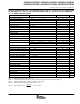
PACKAGE MATERIALS INFORMATION www.ti.com 16-Aug-2012 TAPE AND REEL INFORMATION *All dimensions are nominal Device UCC28C40DGKR Package Package Pins Type Drawing VSSOP SPQ Reel Reel A0 Diameter Width (mm) (mm) W1 (mm) B0 (mm) K0 (mm) P1 (mm) W Pin1 (mm) Quadrant DGK 8 2500 330.0 12.4 5.3 3.4 1.4 8.0 12.0 Q1 UCC28C40DR SOIC D 8 2500 330.0 12.4 6.4 5.2 2.1 8.0 12.0 Q1 UCC28C41DGKR VSSOP DGK 8 2500 330.0 12.4 5.3 3.4 1.4 8.0 12.
PACKAGE MATERIALS INFORMATION www.ti.com 16-Aug-2012 Device Package Package Pins Type Drawing SPQ Reel Reel A0 Diameter Width (mm) (mm) W1 (mm) B0 (mm) K0 (mm) P1 (mm) W Pin1 (mm) Quadrant UCC38C43DR SOIC D 8 2500 330.0 12.4 6.4 5.2 2.1 8.0 12.0 Q1 UCC38C44DGKR VSSOP DGK 8 2500 330.0 12.4 5.3 3.4 1.4 8.0 12.0 Q1 UCC38C44DR SOIC D 8 2500 330.0 12.4 6.4 5.2 2.1 8.0 12.0 Q1 UCC38C45DGKR VSSOP DGK 8 2500 330.0 12.4 5.3 3.4 1.4 8.0 12.
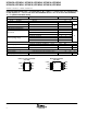
PACKAGE MATERIALS INFORMATION www.ti.com 16-Aug-2012 Device Package Type Package Drawing Pins SPQ Length (mm) Width (mm) Height (mm) UCC38C40DGKR VSSOP DGK 8 2500 367.0 367.0 35.0 UCC38C40DR SOIC D 8 2500 340.5 338.1 20.6 UCC38C41DR SOIC D 8 2500 340.5 338.1 20.6 UCC38C42DGKR VSSOP DGK 8 2500 367.0 367.0 35.0 UCC38C42DR SOIC D 8 2500 340.5 338.1 20.6 UCC38C43DGKR VSSOP DGK 8 2500 367.0 367.0 35.0 UCC38C43DR SOIC D 8 2500 340.5 338.1 20.
IMPORTANT NOTICE Texas Instruments Incorporated and its subsidiaries (TI) reserve the right to make corrections, enhancements, improvements and other changes to its semiconductor products and services per JESD46, latest issue, and to discontinue any product or service per JESD48, latest issue. Buyers should obtain the latest relevant information before placing orders and should verify that such information is current and complete.