
Datasheet

DN-87
Design Note
INTRODUCTION
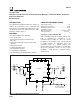
The UCC3918 evaluation kit allows the designer to
evaluate the performance of the UCC3918 Low
On-Resistance Hot Swap Power Manager in a typi-
cal application circuit. The schematic for the evalu-
ation kit is shown in Figure 1.
FEATURES
•
Integrated 0.06Ω Power MOSFET
•
3V to 6V Operation
•
External Analog Control of Fault Current
0A to 4A
•
Independent Analog Control of Current Limit
up to 5A
•
Overload Protection
• 1µA ICC when Disabled
• Programmable On Time
• Programmable Start Delay
• Fixed 3% Duty Cycle During Fault Conditions
ABSOLUTE MAXIMUM RATINGS
Input Supply Voltage . . . . . . . . . . . . . . . . . . . . . . . . . 8V
SOIC Power Dissipation. . . . . . . . . . . . . . . . . . . . . 2.5W
Fault Output Sink Current. . . . . . . . . . . . . . . . . . . 50mA
Fault Output Voltage . . . . . . . . . . . . . . . . . . . . . . . . . V
IN
Output Current (DC) . . . . . . . . . . . . . . Internally Limited
TTL Input Voltage. . . . . . . . . . . . . . . . . . . . .–0.3V to V
IN
Functions of SW1, SW2 and SW3
SW1 and SW2 provide the designer with the flexi-
bility of evaluating the performance of the
UCC3918 when residing on either the system
backplane or on an adapter card. Closing SW1 af-
ter SW2 simulates an application where the
UCC3918 resides on a plug-in adapter card.
Closing SW1 prior to SW2 simulates an application
where the UCC3918 resides on the system
backplane. SW3 provides a shutdown input to
disable the IC.
03/99
UCC3918 “Low On-Resistance Hot Swap Power Manager”, Evaluation Board, Schematic,
and List of Materials
By Dave Olson
7
15
16
14
V
OUT
SHTDWN
C4 SW3
R5
V
IN
C3
TB2
+
–
SW2
513124
98
R2
R3
R4
C5
V
IN
OPTIONAL SOURCING
DELAY COMPONENTS
I
MAX
I
FAULT
10 CT
C2
6
FAULT
3
2
1
V
IN
C1
R1
TB1
+
–
V
IN
UCC3918
V
IN
V
IN
V
OUT
V
OUT
SW1
D1
Figure 1. UCC3918 Evaluation Board Schematic
UDG-98046