
Datasheet
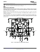
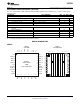
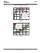

BP3GND
T
MON
V
IN
PWM-B
SRE-B
FLT-B
V DIS
GG
I -B
MON
BST-B
BSW-B
SW-B
PGND
PWM-A
SRE-A
FLT-A
I -A
MON
BST-A
BSW-A
SW-A
PGND
V
GG
UCD7242
www.ti.com
SLUS962B –JANUARY 2010–REVISED AUGUST 2012
Digital Dual Synchronous-Buck Power Driver
Check for Samples: UCD7242
1
FEATURES
APPLICATIONS
• Fully Integrated Power Switches With Drivers • Digitally-Controlled Synchronous-Buck Power
for Dual Synchronous Buck Converters Stages
• Full Compatibility With TI Fusion Digital Power • High Current Dual-Phase VRM/EVRD
Supply Controllers, Such as the UCD92xx Regulators for Desktop, Server, Telecom and
Family Notebook Processors
• Wide Input Voltage Range: 4.75 V to 18 V
Operational Down to 2.2 V Input With an
External Bias Supply
• Up to 10A Output Current per Channel
• Operational to 2 MHz Switching Frequency
• High Side Current Limit With Current Limit
Flag
• Onboard Regulated 6 V Driver Supply From V
IN
• Thermal Protection
• Temperature Sense Output – Voltage
Proportional to Chip Temperature
• UVLO and OVLO Circuits Ensure Proper Drive
Voltage
• Rated From –40°C to 125°C Junction
Temperature
• RoHS Compliant
• Accurate On-Die Current Sensing (±5%)
DESCRIPTION
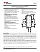
The UCD7242 is a complete power system ready to drive two independent buck power supplies (see Figure 1).
High side MOSFETs, low side MOSFETs, drivers, current sensing circuitry and necessary protection functions
are all integrated into one monolithic solution to facilitate minimum size and maximum efficiency. Driver circuits
provide high charge and discharge current for the high-side NMOS switch and the low-side NMOS synchronous
rectifier in a synchronous buck circuit. The MOSFET gates are driven to +6.25 V by an internally regulated V
GG
supply. The internal V
GG
regulator can be disabled to permit the user to supply an independent gate drive
voltage. This flexibility allows a wide power conversion input voltage range of 2.2V to 18V. Internal under voltage
lockout (UVLO) logic ensures V
GG
is good before allowing chip operation.
The synchronous rectifier enable (SRE) pin controls whether or not the low-side MOSFET is turned on when the
PWM signal is low. When SRE is high the part operates in continuous conduction mode for all loads. In this
mode the drive logic block uses the PWM signal to control both the high-side and low-side gate drive signals.
Dead time is also optimized to prevent cross conduction. When SRE is low, the part operates in discontinuous
conduction mode at light loads. In this mode the low-side MOSFET is always held off.
1
Please be aware that an important notice concerning availability, standard warranty, and use in critical applications of
Texas Instruments semiconductor products and disclaimers thereto appears at the end of this data sheet.
PRODUCTION DATA information is current as of publication date.
Copyright © 2010–2012, Texas Instruments Incorporated
Products conform to specifications per the terms of the Texas
Instruments standard warranty. Production processing does not
necessarily include testing of all parameters.