
Datasheet

VOLTAGE REFERENCE
VOLTAGE MONITORING
RAIL SHUTDOWN
UCD9080
SLVS692E – SEPTEMBER 2006 – REVISED MAY 2008 ...................................................................................................................................................
www.ti.com
The user must consider GPO polarity usage when programming the UCD9080 I
2
C address using the external
GPOx (ADDRx) resistor networks. Acceptable ADDRx bit voltage levels are set according to Schmitt-trigger input
specifications. The following GPOx/ADDRx combinations are acceptable:
• GPOx = Active-low polarity: Corresponding ADDRx bit set to Schmitt-trigger input logic level = 1
• GPOx = Active-high polarity: Corresponding ADDRx bit set to Schmitt-trigger input logic level = 0
The UCD9080 has a voltage reference that is selectable via the I
2
C interface and parameter configuration
section. The voltage reference can either be an internally generated 2.5-V reference or an external 3.3-V
reference. If the external voltage reference is selected, then the 3.3-V reference is from the V
CC
supply to the
UCD9080.
Depending on the voltage reference that is being used, the accuracy of reading voltages is affected. The internal
reference is not as accurate as the external reference and affects the accuracy of the sampled voltages of the
monitored rails. See the Electrical Characteristics for information on voltage reading accuracy for use with each
of the references.
The Configuring the UCD9080 section details how to select the internal or external voltage reference.
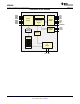
The UCD9080 can monitor eight voltage rails through the MONx terminals of the device (MON1 – MON8). The
UCD9080 samples these eight input channels using either the internal 2.5-V reference or V
CC
(3.3 V) as a
voltage reference to convert the voltage to digital values. The eight digitally monitored voltage values are
accessible via the I
2
C interface.
When monitoring a voltage rail that has a nominal voltage larger than 2.5 V (internal reference) or 3.3 V (external
reference), a resistor divider network is typically used. The design must ensure that the source impedance of that
resistor network is not too high, because it causes the UCD9080 analog-to-digital converter (ADC) to take longer
to perform the sample-and-hold conversion. The extended conversion time causes the frequency of the sampling
of voltage rails to slow below 20 kHz.
Using a higher-valued resistor network lowers the overall power dissipation of the solution, which is desirable. In
order to keep the source impedance low, a buffer circuit is typically used. The UCD9080 analog inputs require
that a source impedance of less than 20 k Ω be used in order to maintain the high sampling rate of the voltages.
The UCD9080 allows specification of overvoltage threshold, undervoltage threshold, and out-of-regulation or
glitch duration for each monitored rail.
Each voltage rail can also be marked so that it is not monitored, in which case all checks and alarm conditions
are disabled.
Rail shutdown is the act of setting the ENx pin associated with that rail to a state which disables the power
supply output. Each UCD9080 rail can be configured to shut down based on a monitored alarm event (sustained
overvoltage, sustained undervoltage, or rail did not start) and in a configurable manner.
The options for rail shutdown are as follows:
• Ignore
• Log only
• Sequence
• Retry 1 time
• Retry 0 times
If the system does not care whether a monitored rail enters a sustained error condition, the UCD9080 can be
configured to either ignore or log the error event and take no subsequent action.
10 Submit Documentation Feedback Copyright © 2006 – 2008, Texas Instruments Incorporated
Product Folder Link(s) :UCD9080