
Datasheet
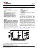

ORDERING INFORMATION
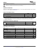
ABSOLUTE MAXIMUM RATINGS
(1)
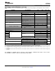
RECOMMENDED OPERATING CONDITIONS
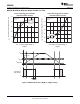
ELECTRICAL CHARACTERISTICS
UCD9080
SLVS692E – SEPTEMBER 2006 – REVISED MAY 2008 ...................................................................................................................................................
www.ti.com
These devices have limited built-in ESD protection. The leads should be shorted together or the device placed in conductive foam
during storage or handling to prevent electrostatic damage to the MOS gates.
For the most current package and ordering information, see the Package Option Addendum at the end of this
document, or see the TI Web site at www.ti.com .
VALUE UNIT
Voltage applied from VCC to VSS – 0.3 to 4.1 V
Voltage applied to any pin
(2)
– 0.3 to V
CC
+ 0.3 V
Diode current at any device terminal ± 2 mA
T
stg
Storage temperature – 40 to 85 ° C
(1) Stresses beyond those listed under absolute maximum ratings may cause permanent damage to the device. These are stress ratings
only and functional operation of the device at these or any other conditions beyond those indicated under recommended operating
conditions is not implied. Exposure to absolute-maximum-rated conditions for extended periods may affect device reliability.
(2) All voltages referenced to VSS.
MIN NOM MAX UNIT
Supply voltage during operation 3 3.3 3.6
V
CC
V
Supply voltage during configuration changes 3 3.3 3.6
T
A
Operating free-air temperature range – 40 85 ° C
These specifications are over recommended ranges of supply voltage and operating free-air temperature, unless otherwise
noted
PARAMETER TEST CONDITIONS MIN NOM MAX UNIT
SUPPLY CURRENT
Supply current into V
CC
, excluding external
I
S
T
A
= 25 ° C 3 4 mA
current
I
C
Supply current during configuration 3.6 V 3 7 mA
STANDARD INPUTS (RST, TEST)
V
IL
Low-level input voltage V
CC
= 3 V V
SS
V
SS
+ 0.6 V
V
IH
High-level input voltage V
CC
= 3 V 0.8 V
CC
V
CC
V
SCHMITT TRIGGER INPUTS (SDA, SCL, EN1, EN2, EN3, EN4, EN5, EN6, EN7, EN8/ADDR1, ADDR2, ADDR3, ADDR4)
V
IT+
Positive-going input threshold voltage V
CC
= 3 V 1.5 1.9 V
V
IT –
Negative-going input threshold voltage V
CC
= 3 V 0.9 1.3 V
V
hys
Input-voltage hysteresis, (V
IT+
– V
IT –
) V
CC
= 3 V 0.5 1 V
I
lkg
High-impedance leakage current ± 50 nA
2 Submit Documentation Feedback Copyright © 2006 – 2008, Texas Instruments Incorporated
Product Folder Link(s) :UCD9080