
Datasheet

UCD9080
www.ti.com
................................................................................................................................................... SLVS692E – SEPTEMBER 2006 – REVISED MAY 2008
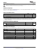
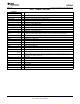
ELECTRICAL CHARACTERISTICS (continued)
These specifications are over recommended ranges of supply voltage and operating free-air temperature, unless otherwise
noted
PARAMETER TEST CONDITIONS MIN NOM MAX UNIT
ANALOG INPUTS (MON1, MON2, MON3, MON4, MON5, MON6, MON7, MON8, ROSC)
V
CC
Analog supply voltage V
SS
= 0 V 3 3.6 V
Internal voltage reference 0 2.5
V
(R<1..8>)
Analog input voltage V
External voltage reference
0 V
CC
(V
CC
= 3.3 V used as reference)
Only one terminal can be selected at a time
C
I
(1)
Input capacitance 27 pF
(MON1 – MON8)
Input MUX ON resistance 0 V ≤ V
(MONx)
≤ VCC, V
CC
= 3 V 2000 Ω
R
I
(1)
I
lkg
High-impedance leakage current MON1 – MON8 ± 50 nA
REF2_5V = 1 for 2.5 V I
(VREF+)
≤
VREF+ Positive internal reference voltage output 2.35 2.5 2.65 V
I
(VREF+)
max, V
CC
= 3 V
REF2_5V = 1, I
(VREF+)
≤ 0.5 mA 3 V
VCC minimum voltage, positive built-in
V
CC
(min)
reference active
REF2_5V = 1, I
(VREF+)
≤ 1 mA 3 V
Internal reference (2.5 V) ± 6.8 ± 12 ± 17.4
V
(acc)
Accuracy of voltage sampling from rails mV
External reference (3.3 V/V
CC
) ± 0.2 ± 1.6 ± 6.8
Temperature coefficient of built-in I
(VREF+)
is a constant in the range of
± 100 ppm/ ° C
T
REF+
(1)
reference 0 mA ≤ I
(VREF+)
≤ 1 mA, VCC = 3 V
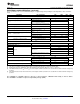
MISCELLANEOUS
t
retention
Retention of configuration parameters T
J
= 25 ° C 100 Years
POR, Brownout, Reset
(2) (3)
t
d(BOR)
2000 µ s
VCC
(start)
0.7 × V
(B_IT – )
V
V
(B_IT – )
VCC/dt ≤ 3 V/s 1.71 V
Brownout
V
hys(B_IT – )
70 130 180 mV
Pulse length needed at RST pin to accept
t
(reset)
2 µ s
reset internally, V
CC
= 3 V
DIGITAL OUTPUTS (EN8/GPO1, GPO2, GPO3, GPO4, EN1, EN2, EN3, EN4, EN5, EN6, EN7, SDA, SCL )
I
OH
(max) = – 1.5 mA,
(4)
V
CC
= 3 V V
CC
– 0.25 V
CC
V
OH
High-level output voltage V
I
OH
(max) = – 6 mA,
(5)
V
CC
= 3 V V
CC
– 0.6 V
CC
I
OH
(max)= – 1.5 mA,
(4)
V
CC
= 3 V V
SS
V
SS
+ 0.25
V
OL
Low-level output voltage V
I
OH
(max) = – 6 mA,
(5)
V
CC
= 3 V V
SS
V
SS
+ 0.6
I
lkg
High-impedance leakage current V
CC
= 3 V ± 50 nA
(1) Not production tested. Limits verified by design.
(2) The current consumption of the brownout module is already included in the I
CC
current-consumption data.
(3) During power up, device initialization starts subsequent to a period of t
d(BOR)
after V
CC
= V
(B_IT – )
+ V
hys(B_IT – )
.
(4) The maximum total current, I
OH
max and I
OL
max, for all outputs combined, should not exceed ± 12 mA to hold the maximum voltage drop
specified.
(5) The maximum total current, I
OH
max and I
OL
max, for all outputs combined, should not exceed ± 48 mA to hold the maximum voltage drop
specified.
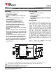
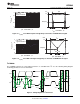
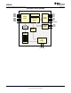
The UCD9080 is compatible with 3.3-V IO ports of microcontrollers, TMS320™ DSP family as well as ASICs.
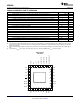
The UCD9080 is available in a plastic 32-pin QFN package (RHB).
Copyright © 2006 – 2008, Texas Instruments Incorporated Submit Documentation Feedback 3
Product Folder Link(s) :UCD9080