
Datasheet

V =3V
TypicalConditions
CC
V
V
C
C(min)
-
t PulseWidth S
pw
- - m
t PulseWidth S
pw
- - m
t
pw
V
CC
V
CC(min)
3V
1ns
2
1
1.5
1000
0
0.5
0.001
1
1ns
V =3V
TypicalConditions
CC
V
V
CC(min)
-
t PulseWidth S
pw
- - m
t PulseWidth s
pw
- - m
t
pw
t t
fall
=
rise
t
fall
t
rise
V
CC
V
CC(min)
3V
2
1
1.5
1000
0
0.5
0.001
1
I
2
C TIMING
S
SDA
SCL
SPSr
t
r
t
SU;STO
t
BUF
t
HD;STA
t
SU;STA
t
r
t
HIGH
t
HD;DAT
t
SU;DAT
t
HD;STA
t
LOW
t
f
t
of
UCD9080
www.ti.com
................................................................................................................................................... SLVS692E – SEPTEMBER 2006 – REVISED MAY 2008
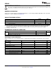
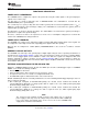
Figure 5. V
CC(min)
Level With a Square Voltage Drop to Generate a POR/Brownout Signal
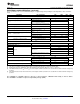
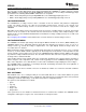
Figure 6. V
CC(min)
Level With a Triangle Voltage Drop to Generate a POR/Brownout Signal
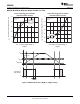
The UCD9080 supports the same timing parameters as standard-mode I
2
C. See the following timing diagram
and timing parameters for more information.
Figure 7. Timing Diagram for I
2
C Interface
Copyright © 2006 – 2008, Texas Instruments Incorporated Submit Documentation Feedback 5
Product Folder Link(s) :UCD9080