
Datasheet
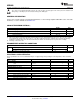
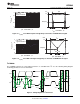
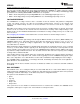

TIMING PARAMETERS FOR I
2
C INTERFACE
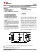
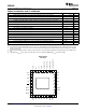
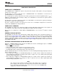
VSS
NC
XIN
NC
RST
MON1
MON2
MON3
EN2
EN1
SCL
SDA
NC
MON5
MON4
NC
1
2
3
4
5
6
7
8
24
23
22
21
20
19
18
17
10 11 12 13 14 15 169
25272829303132 26
ROSC
NC
VCC
TEST
ADDR4/GPO4
ADDR2/GPO2
ADDR3/GPO3
MON6
EN4
EN3
EN5
EN6
EN7
MON7
MON8
EN8/ADDR1/GPO1
UCD9080
SLVS692E – SEPTEMBER 2006 – REVISED MAY 2008 ...................................................................................................................................................
www.ti.com
PARAMETER MIN MAX UNIT
t
of
Output fall time from V
OH
to V
OL
(1)
with a bus capacitance from 10 pF to 400 pF 250
(2)
ns
C
I
Capacitance for each pin. 10 pF
f
SCL
SCL clock frequency 10 100 kHz
t
HD;STA
Hold time (repeated) START condition. After this period, the first clock pulse is generated. 4 µ s
t
HD;DAT
Data hold time 0
(3)
3.45
(4)
µ s
t
LOW
LOW period of the SCL clock 4.7 µ s
t
HIGH
HIGH period of the SCL clock 4 µ s
t
SU;STA
Set-up time for repeated start condition 4.7 µ s
t
SU;DAT
Data setup time 250 ns
t
r
Rise time of both SDA and SCL signals 1000 ns
t
f
Fall time of both SDA and SCL signals 300 ns
t
SU;STO
Setup time for STOP condition 4 µ s
t
BUF
Bus free time between a STOP and START condition 4.7 µ s
C
(b)
Capacitive load for each bus line 400 pF
V
nL
Noise margin at the LOW level for each connected device (including hysteresis) 0.1 VDD V
V
nH
Noise margin at the HIGH level for each connected device (including hysteresis) 0.2 VDD V
(1) See the Electrical Characteristics section of this data sheet.
(2) The maximum t
f
for the SDA and SCL bus lines (300 ns) is longer than the specified maximum t
of
for the output stages (250 ns). This
allows series protection resistors (R
s
) to be connected between the SDA/SCL pins and the SDA/SCL bus lines without exceeding the
maximum specified t
f
.
(3) A device must internally provide a hold time of at least 300 ns for the SDA signal to bridge the undefined region of the falling edge of
SCL.
(4) The maximum t
HD;DAT
must only be met if the device does not stretch the LOW period (t
LOW
) of the SCL signal.
RHB PACKAGE
(TOP VIEW)
6 Submit Documentation Feedback Copyright © 2006 – 2008, Texas Instruments Incorporated
Product Folder Link(s) :UCD9080