
Datasheet

UCD9080
www.ti.com
................................................................................................................................................... SLVS692E – SEPTEMBER 2006 – REVISED MAY 2008
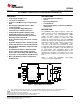
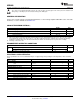
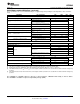
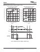
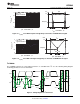
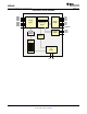
Table 1. TERMINAL FUNCTIONS
TERMINAL
I/O DESCRIPTION
NAME NO.
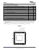
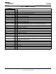
ADDR2/GPO2 26 I/O I
2
C address select 2, general-purpose digital output 2
ADDR3/GPO3 27 I/O I
2
C address select 3, general-purpose digital output 3
ADDR4/GPO4 28 I/O I
2
C address select 4, general-purpose digital output 4
EN1 23 I/O Voltage rail 1 enable (digital output)
EN2 24 I/O Voltage rail 2 enable (digital output)
EN3 11 I/O Voltage rail 3 enable (digital output)
EN4 10 I/O Voltage rail 4 enable (digital output)
EN5 12 I/O Voltage rail 5 enable (digital output)
EN6 13 I/O Voltage rail 6 enable (digital output)
EN7 14 I/O Voltage rail 7 enable (digital output)
EN8/ADDR1/
25 I/O Voltage rail 8 enable (digital output), I
2
C address select 1, general-purpose digital output 1
GPO1
MON1 6 I Analog input for voltage rail 1
MON2 7 I Analog input for voltage rail 2
MON3 8 I Analog input for voltage rail 3
MON4 18 I Analog input for voltage rail 4
MON5 19 I Analog input for voltage rail 5
MON6 9 I Analog input for voltage rail 6
MON7 15 I Analog input for voltage rail 7
MON8 16 I Analog input for voltage rail 8
NC 2 Do not connect.
4,17,
NC Not connected internally. Connect to VSS.
20, 31
Internal oscillator frequency adjust. Must use 100-k Ω pullup to VCC for minimum drift and maximum
ROSC 32
frequency when sampling voltage rails.
RST 5 I Reset input
SCL 22 I/O I
2
C clock. A pullup rwesistor to 3.3 V is required.
SDA 21 I/O I
2
C data (bidirectional). A pullup resistor to 3.3 V is required.
TEST 29 I Connect to VSS
VCC 30 Supply voltage
VSS 1 Ground reference
XIN 3 Connect to VCC
Copyright © 2006 – 2008, Texas Instruments Incorporated Submit Documentation Feedback 7
Product Folder Link(s) :UCD9080