
Datasheet

FUNCTIONAL DESCRIPTION
POWER-SUPPLY SEQUENCING
POWER-SUPPLY ENABLES
GENERAL-PURPOSE OUTPUTS
EXTERNAL CONSIDERATIONS FOR EN AND GPO PINS
UCD9080
www.ti.com
................................................................................................................................................... SLVS692E – SEPTEMBER 2006 – REVISED MAY 2008
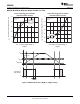
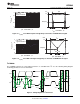
The UCD9080 can be configured to sequence the power rails using the enable signals or the general-purpose
outputs in one of three ways.
The first way is to specify a delay time after a UCD9080 RESET. The enable/GPO is asserted after the
UCD9080 RESET plus a specified delay.
The second way is to specify a delay time after another (parent) rail has achieved regulation (that is, V
RAIL
is
within the specified under- and overvoltage settings). The enable/GPO is asserted after the (parent) rail is in
regulation plus specified delay.
The third way is to specify a (parent) rail voltage. The enable/GPO is asserted after the (parent) rail voltage is
greater than or equal to the specified voltage.
Of course, a rail does not have to be sequenced, as in the case of a backplane voltage that is not under the
control of the UCD9080, but is being monitored.
The UCD9080 can sequence up to eight power supplies using the ENx (EN1 to EN8) signals. These signals can
be configured as active-high or active-low, supporting power supplies with either polarity.
EN8 can also be configured as a GPO (GPO1). EN8/ADDR1/GPO1 is also used for I
2
C address selection
(ADDR1).
The UCD9080 can control up to four general-purpose digital outputs using the same sequencing mechanisms as
described in the Power-Supply Enables section. These general-purpose outputs (referred to as GPO1 – GPO4)
can be used for digital signals such as RESET or status. Note that these signals are multiplexed with other
functions (primarily I
2
C address selection). See the Terminal Functions table to ensure that these signals are
used properly by the application. Also note that the GPO1 signal is multiplexed with EN8, so both of these cannot
be used at the same time.
During the UCD9080 RESET interval, all ENx and GPOx pins become Schmitt-trigger Inputs. A UCD9080
RESET occurs under the following conditions:
• External RST pin is driven low.
• Power is applied to the device (power-on reset) or power is cycled.
• A sequence event occurs as a result of a configured rail-alarm event.
• The RESTART register is written with a value of 0 over the I
2
C bus.
All ENx and GPOx pins must be externally terminated to one of the following Schmitt-trigger input-logic states for
proper sequencer operation.
• EN or GPO pin configured for ACTIVE-LOW polarity: the external resistor network must default the
corresponding EN or GPO pin to a voltage greater than or equal to 1.9 V (V
IT+
, MAX, positive-going input
threshold voltage) during device reset.
• EN or GPO pin configured for ACTIVE-HIGH polarity: the external resistor network must default the
corresponding EN or GPO pin to a voltage less than or equal to 0.9 V (V
IT –
, MIN, negative-going input
threshold voltage) during device reset.
NOTE:
The external resistor networks should not derive their voltage from a sequenced
power supply, as this may cause the voltage level presented to the ENx or GPOx pin
to be at the wrong level during device reset. It is best to use the UCD9080 VCC
supply for the external resistor networks.
Copyright © 2006 – 2008, Texas Instruments Incorporated Submit Documentation Feedback 9
Product Folder Link(s) :UCD9080