
Datasheet
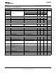
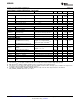


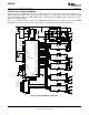
Table Of Contents
- FEATURES
- APPLICATIONS
- DESCRIPTION
- ELECTRICAL SPECIFICATIONS
- ABSOLUTE MAXIMUM RATINGS
- RECOMMENDED OPERATING CONDITIONS
- ELECTRICAL CHARACTERISTICS
- ADC MONITORING INTERVALS AND RESPONSE TIMES
- HARDWARE FAULT DETECTION LATENCY
- PMBus/SMBus/I2C
- I2C/SMBus/PMBus Timing Characteristics
- FUNCTIONAL OVERVIEW
- PMBus Interface
- Resistor Programmed PMBus Address Decode
- JTAG Interface
- Bias Supply Generator (Series Regulator Controller)
- Power On Reset
- External Reset
- Output Voltage Adjustment
- Analog Front End (AFE)
- Digital Compensator
- DPWM Engine
- Flexible Rail/Power Stage Configuration
- DPWM Phase Distribution
- DPWM Synchronization
- Phase Shedding at Light Current Load
- Phase Adding at Normal Current Load
- Output Current Measurment
- Output Current Balancing
- Overcurrent Detection
- Current Foldback Mode
- Input Voltage and Current Monitoring
- Temperature Monitoring
- Temperature Balancing
- Soft Start, Soft Stop Ramp Sequence
- Input UV Lockout
- Voltage Tracking
- Sequencing
- Fan Control
- Non-volatile Memory Error Correction Coding
- APPLICATION INFORMATION

TYPICAL APPLICATION SCHEMATIC
–Vsens-rail3
10kW
0.1 mF
FCX491A
+3.3V
UCD9240RGC
53
52
51
50
57
56
55
54
47
44
7
45
3
59
60
61
62
63
1
2
EAp1
EAn2
EAp2
EAn1
EAn4
EAp4
EAn3
EAp3
AddrSens1
AddrSens0
CS-1A(COMP1)
CS-2A(COMP2)
CS-2B
CS-1B
CS-4A(COMP4)
CS-3A(COMP3)
+Vsens-rail1
–Vsens-rail2
+Vsens-rail2
–Vsens-rail1
–Vsens-rail4
+Vsens-rail4
+Vsens-rail3
CS-rail2B
CS-rail1A
CS-rail4A
CS-rail3A
CS-rail2A
CS-rail1B
6
5
4
Temp
Vtrack
Vin/Iin
16
15
PMBus-Data
PMBus-Clk
39
28
27
PowerGood(TMS)
PMBus-Ctrl
PMBus-Alert
+3.3V
46
52
V33FB
V33A
V33D
V33DIO-1
V33DIO-2
BPCap
4.7 mF
20
19
18
17
12
11
23
21
DPWM-1A
15kW
0.1 mF
34
25
14
13
24
22
35
33
30
29
32
31
42
FAN-Tach
36
41
FAN-PWM
SyncOut
37
38
SyncIn
10
40
DPWM-2B
DPWM-2A
DPWM-1B
FAULT-1B
FAULT-1A
DPWM-4A
DPWM-3A
FAULT-2A
FAULT-4A
FAULT-3A
FAULT-2B
SRE-1B
SRE-1A
SRE-2B
SRE-2A
SRE-4A
SRE-3A
TMUX-1
TMUX-0
TMUX-2
FAN-TACH
FAN-PWM
SYNC-OUT
SYNC-IN
RCR
TRST
9
RESET
10kW
10kW
V
IN
49
48
64
8
26
Dgnd-2
Dgnd-1
Agnd-3
Agnd-2
Agnd-1
43
Dgnd-3
10kW
14
13
A1
A0
1
12
15
A4
A3
A2
4
2
A7
A6
A5
5
8
11
10
6
S2
Com
S0
S1
EN
3
Temp-rail1B
Temp-rail1A
Temp-rail2B
Temp-rail2A
Temp-rail4A
Temp-rail3A
CD74HC4051
+3.3V
16
PTD08A010W
FAULT
PWM
SRE
INH IOUT
PTD08A010W
FAULT
PWM
SRE
INH IOUT
Commutation
UCD7230Driver
Logic
FAULT
PWM
SRE
INH
IOUT
TempSensor
PTD08A020W
Temp-rail1A
INH
+3.3V
V
IN
V
O
PTD08A020W
FAULT
PWM
SRE
INH IOUT
Temp-rail1B
CS-rail1A
+Vsens-rail1
–Vsens-rail1
Temp-rail2A
Temp-rail2B
+Vsens-rail2
–Vsens-rail2
CS-rail1B
CS-rail2A
CS-rail2B
PTD08A010W
FAULT
PWM
SRE
INH IOUT
PTD08A010W
FAULT
PWM
SRE
INH IOUT
Temp-rail3A
Temp-rail4A
+Vsens-rail4
–Vsens-rail4
CS-rail3A
CS-rail4A
+Vsens-rail3
–Vsens-rail3
82.5kW
TEMP
VOUT
GND
VBIAS
TEMP
GND
TEMP
VOUT
GND
TEMP
VOUT
GND
TEMP
VOUT
GND
TEMP
VOUT
GND
VBIAS VIN
VIN
VBIAS VIN
VIN
VBIAS VIN
VIN
VBIAS VIN
VIN
VBIAS VIN
VIN
[A]
UDG-08035
UCD9240
SLUS766C – JULY 2008 – REVISED NOVEMBER 2008 ...................................................................................................................................................
www.ti.com
Figure 3 shows the UCD9240 power supply controller as part of a system that provides the regulation of four
independent power supplies. The loop for each power supply is created by the respective voltage outputs feeding
into the differential voltage error ADC (EADC) inputs, and completed by DPWM outputs feeding into the gate
drivers for each power stage.
The ± V
sense
rail signals must be routed to the EAp/EAn input that matches the number of the lowest DPWM
configured as part of the rail. (See more detail on page 19, " Flexible Rail/Power Stage Configuration " .)
Figure 3. Typical Application Schematic
10 Submit Documentation Feedback Copyright © 2008, Texas Instruments Incorporated
Product Folder Link(s): UCD9240