
Datasheet
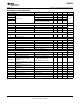
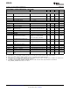


Table Of Contents
- FEATURES
- APPLICATIONS
- DESCRIPTION
- ELECTRICAL SPECIFICATIONS
- ABSOLUTE MAXIMUM RATINGS
- RECOMMENDED OPERATING CONDITIONS
- ELECTRICAL CHARACTERISTICS
- ADC MONITORING INTERVALS AND RESPONSE TIMES
- HARDWARE FAULT DETECTION LATENCY
- PMBus/SMBus/I2C
- I2C/SMBus/PMBus Timing Characteristics
- FUNCTIONAL OVERVIEW
- PMBus Interface
- Resistor Programmed PMBus Address Decode
- JTAG Interface
- Bias Supply Generator (Series Regulator Controller)
- Power On Reset
- External Reset
- Output Voltage Adjustment
- Analog Front End (AFE)
- Digital Compensator
- DPWM Engine
- Flexible Rail/Power Stage Configuration
- DPWM Phase Distribution
- DPWM Synchronization
- Phase Shedding at Light Current Load
- Phase Adding at Normal Current Load
- Output Current Measurment
- Output Current Balancing
- Overcurrent Detection
- Current Foldback Mode
- Input Voltage and Current Monitoring
- Temperature Monitoring
- Temperature Balancing
- Soft Start, Soft Stop Ramp Sequence
- Input UV Lockout
- Voltage Tracking
- Sequencing
- Fan Control
- Non-volatile Memory Error Correction Coding
- APPLICATION INFORMATION

ELECTRICAL CHARACTERISTICS
UCD9240
www.ti.com
................................................................................................................................................... SLUS766C – JULY 2008 – REVISED NOVEMBER 2008
PARAMETER TEST CONDITIONS MIN NOM MAX UNIT
SUPPLY CURRENT
I
V33A
V
V33A
= 3.3 V 8 15
I
V33DIO
V
V33DIO
= 3.3 V 2 10
Supply current mA
I
V33D
V
V33D
= 3.3 V 40 45
V
V33D
= 3.3 V storing configuration
I
V33D
50 55
parameters in flash memory TBD
INTERNAL REGULATOR CONTROLLER INPUTS/OUTPUTS
V
V33
3.3-V linear regulator Emitter of NPN transistor 3.25 3.3 3.35
V
V33FB 3.3-V linear regulator feedback 4 4.6
I
V33FB
Series pass base drive V
VIN
= 12 V 10 mA
Beta Series NPN pass device 40
EXTERNALLY SUPPLIED 3.3 V POWER
V
V33D
,
Digital 3.3-V power T
A = 25 ° C
3.13 3.47 V
V
V33DION
V
V33A
Analog 3.3-V power T
A = 25 ° C
3.13 3.47 V
ERROR AMPLIFIER INPUTS EAPn, EANn
V
CM
Common mode voltage each pin -0.15 1.848 V
V
DIFF
Differential Voltage Range -0.256 1.998 V
V
ERROR
Internal error Voltage range AFE_GAIN field of CLA_GAINS = 0
(1)
-256 248 mV
EAP-EAN Error voltage digital resolution AFE_GAIN field of CLA_Gains = 3 1 mV
R
EA
Input Impedance Ground reference 0.5 1.5 3 M Ω
I
OFFSET
Input offset current 1 k Ω source impedence -5 5 µ A
ANALOG INPUTS CS, V
in
, TEMP, PMBusADDR
I
BIAS
Bias current for PMBus Addr pins 9 11 µ A
V
ADDR_OPEN
Voltage indicating open pin AddrSens 0,1 open 2.47 V
V
ADDR_SHORT
Voltage indicating shorted pin AddrSense 0,1 short to ground 0.179 V
Inputs: V
In
, V
track
, V
temp
Measurment range for voltage
V
ADC_RANGE
CS-1A, CS-1B, CS-2A, CS-2B 0 2.5 V
monitoring
CS-3A, CS-3B, CS-4A, CS-4B
Overcurrent comparator threshold
V
OC_THRS
Inputs: CS-1A, CS-2A, CS-3A, CS-4A 0.032 2 V
voltage range
Overcurrent comparator threshold
V
OC_RES
Inputs: CS-1A, CS-2A, CS-3A, CS-4A 31.25 mV
voltage range
ADCREF External Reference input (80-pin package) 1.8 V33A V
Temp
internal
Int. temperature sense accuracy Over range from 0 ° C to 100 ° C -5 5 ° C
INL ADC integral nonlinearity -2.5 2.5 mV
I
lkg
Input leakage current 3V applied to pin 100 nA
R
IN
Input impedance Ground reference 8 M Ω
C
IN
Current Sense Input capacitance 10 pF
(1) See the UCD92xx PMBus Command Reference for the description of the AFE_GAIN field of CLA_GAINS command.
Copyright © 2008, Texas Instruments Incorporated Submit Documentation Feedback 3
Product Folder Link(s): UCD9240