
Datasheet
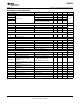
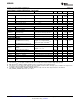
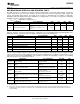


Table Of Contents
- FEATURES
- APPLICATIONS
- DESCRIPTION
- ELECTRICAL SPECIFICATIONS
- ABSOLUTE MAXIMUM RATINGS
- RECOMMENDED OPERATING CONDITIONS
- ELECTRICAL CHARACTERISTICS
- ADC MONITORING INTERVALS AND RESPONSE TIMES
- HARDWARE FAULT DETECTION LATENCY
- PMBus/SMBus/I2C
- I2C/SMBus/PMBus Timing Characteristics
- FUNCTIONAL OVERVIEW
- PMBus Interface
- Resistor Programmed PMBus Address Decode
- JTAG Interface
- Bias Supply Generator (Series Regulator Controller)
- Power On Reset
- External Reset
- Output Voltage Adjustment
- Analog Front End (AFE)
- Digital Compensator
- DPWM Engine
- Flexible Rail/Power Stage Configuration
- DPWM Phase Distribution
- DPWM Synchronization
- Phase Shedding at Light Current Load
- Phase Adding at Normal Current Load
- Output Current Measurment
- Output Current Balancing
- Overcurrent Detection
- Current Foldback Mode
- Input Voltage and Current Monitoring
- Temperature Monitoring
- Temperature Balancing
- Soft Start, Soft Stop Ramp Sequence
- Input UV Lockout
- Voltage Tracking
- Sequencing
- Fan Control
- Non-volatile Memory Error Correction Coding
- APPLICATION INFORMATION

UCD9240
SLUS766C – JULY 2008 – REVISED NOVEMBER 2008 ...................................................................................................................................................
www.ti.com
ELECTRICAL CHARACTERISTICS (continued)
PARAMETER TEST CONDITIONS MIN NOM MAX UNIT
DIGITAL INPUTS/OUTPUTS
Dgnd
V
OL
Low-level output voltage I
OL
= 6 mA
(2)
, V
V33DIO
= 3 V V
+0.25
V
33DIO
V
OH
High-level output voltage I
OH
= -6 mA
(3)
, V
V33DIO
= 3 V V
-0.6V
V
IH
High-level input voltage V
V33DIO
= 3V 2.1 3.6 V
V
IL
Low-level input voltage V
V33DIO
= 3.5 V 1.1 V
FAN CONTROL INPUTS/OUTPUTS
T
PWM_PERIOD
FAN-PWM period 156 kHz
DUTY
PWM
FAN-PWM duty cycle range 0% 100%
DUTY
RES
Duty cycle resolution 1%
For 1 Tach pulse per revolution. At 2,
Tach
RANGE
FAN-TACH range 30 300k RPM
3, or 4 pulse/rev, divide by that value
Tach
RES
FAN-TACH resolution For 1 Tach pulse per revolution 30 RPM
t
MIN
FAN-TACH minimum pulse width Either positive or negative polarity 150 µ s
SYSTEM PERFORMANCE
V
ref
commanded to be 1V, at 25 ° C
V
Ref
Setpoint Reference Accuracy -10 10 mV
AFEgain = 4, 1V input to EAP/N
measured at output of the EADC
(4)
Setpoint Reference Accuracy over
-40 ° C to 125 ° C -20 20 mV
temeprature
AFEgain = 4 compared to
Differential offset between gain
V
DiffOffset
-4 4 mV
setetings
AFEgain = 1, 2, or 8
t
Delay
Digital Compensator Delay
(5)
208
(6)
ns
F
SW
Switching Frequency 15.260 2000 kHz
Duty Max and Min Duty Cycle Configured via PMBus 0% 100%
V
DD
Slew Minimum V
DD
slew rate V
DD
slew rate between 2.3V and 2.9V 0.25 V/ms
t
retention
Retention of configuration parameters T
J
= 25 ° C 100 Years
Number of nonvolatile erase/write
Write_Cycles T
J
= 25 ° C 20 K cycles
cycles
(2) The maximum I
OL
, for all outputs combined, should not exceed 12 mA to hold the maximum voltage drop specified.
(3) The maximum I
OH
, for all outputs combined, should not exceed 48 mA to hold the maximum voltage drop specified.
(4) With default device caliibration. PMBus calibration can be used to improve the regulation tolerance.
(5) Time from close of error ADC sample window to time when digitally calculated control effort (duty cycle) is available. This delay must be
accounted for when calculating the system dynamic response.
(6) The PMBus command: EADC_SAMPLE_TRIGGER defines the start of the 32ns ADC sample window. So the minimum
EAD_SAMPLE_TRIGGER time is 208 + 32 = 240 ns.
4 Submit Documentation Feedback Copyright © 2008, Texas Instruments Incorporated
Product Folder Link(s): UCD9240