
Datasheet
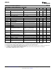
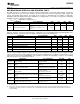

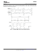


Table Of Contents
- FEATURES
- APPLICATIONS
- DESCRIPTION
- ELECTRICAL SPECIFICATIONS
- ABSOLUTE MAXIMUM RATINGS
- RECOMMENDED OPERATING CONDITIONS
- ELECTRICAL CHARACTERISTICS
- ADC MONITORING INTERVALS AND RESPONSE TIMES
- HARDWARE FAULT DETECTION LATENCY
- PMBus/SMBus/I2C
- I2C/SMBus/PMBus Timing Characteristics
- FUNCTIONAL OVERVIEW
- PMBus Interface
- Resistor Programmed PMBus Address Decode
- JTAG Interface
- Bias Supply Generator (Series Regulator Controller)
- Power On Reset
- External Reset
- Output Voltage Adjustment
- Analog Front End (AFE)
- Digital Compensator
- DPWM Engine
- Flexible Rail/Power Stage Configuration
- DPWM Phase Distribution
- DPWM Synchronization
- Phase Shedding at Light Current Load
- Phase Adding at Normal Current Load
- Output Current Measurment
- Output Current Balancing
- Overcurrent Detection
- Current Foldback Mode
- Input Voltage and Current Monitoring
- Temperature Monitoring
- Temperature Balancing
- Soft Start, Soft Stop Ramp Sequence
- Input UV Lockout
- Voltage Tracking
- Sequencing
- Fan Control
- Non-volatile Memory Error Correction Coding
- APPLICATION INFORMATION

HARDWARE FAULT DETECTION LATENCY
PMBUS/SMBUS/I
2
C
I
2
C/SMBus/PMBus Timing Characteristics
UCD9240
SLUS766C – JULY 2008 – REVISED NOVEMBER 2008 ...................................................................................................................................................
www.ti.com
The controller contains hardware fault detection circuits that are independent of the ADC monitoring sequencer.
PARAMETER TEST CONDITIONS MAX TIME UNIT
15 + 3 ×
Time to disable DPWM output base on active FAULT
t
FAULT
High level on FAULT pin µ s
pin signal
NumPhases
Time to disable the DPWM A output based on internal Step change in CS voltage from 0v to Switch
t
CLF-A
4
analog comparator 2.5V Cycles
Time to disable all remaining DPWM and SRE outputs
10 + 3 ×
Step change in CS voltage from 0V to
t
CLF-B
configured to drive a voltage rail after a CLF-A event µ s
2.5V
NumPhases
occurs
The timing characteristics and timing diagram for the communications interface that supports I
2
C, SMBus and
PMBus are shown below.
T
A
= – 40 ° C to 85 ° C, 3V < V
DD
< 3.6V, typical values at T
A
= 25 ° C and V
CC
= 2.5 V (Unless otherwise noted)
PARAMETER TEST CONDITIONS MIN TYP MAX UNIT
f
SMB
SMBus/PMBus operating frequency Slave mode; SMBC 50% duty cycle 10 1000 kHz
f
I2C
I C operating frequency Slave mode; SCL 50% duty cycle 10 1000 kHz
t
(BUF)
Bus free time between start and stop 4.7 µ s
t
(HD:STA)
Hold time after (repeated) start 0.26 µ s
t
(SU:STA)
Repeated start setup timed 0.26 µ s
t
(SU:STO)
Stop setup time 0.26 µ s
t
(HD:DAT)
Data hold time Receive mode 0 ns
t
(SU:DAT)
Data setup time 50 ns
t
(TIMEOUT)
Error signal/detect See
(1)
35 µ s
t
(LOW)
Clock low period 0.5 µ s
t
(HIGH)
Clock high period See
(2)
0.26 50 µ s
t
(LOW:SEXT)
Cumulative clock low slave extend time See
(3)
25 µ s
t
FALL
Clock/data fall time See
(4)
120 ns
t
RISE
Clock/data rise time See
(5)
120 ns
(1) The UCD9240 times out when any clock low exceeds t
(TIMEOUT)
.
(2) t
(HIGH)
, max, is the minimum bus idle time. SMBC = SMBD = 1 for t > 50 ms causes reset of any transaction involving UCD9240 that is
in progress. This specification is valid when the NC_SMB control bit remains in the default cleared state (CLK[0]=0).
(3) t
(LOW:SEXT)
is the cumulative time a slave device is allowed to extend the clock cycles in one message from initial start to the stop.
(4) Rise time t
RISE
= V
VILMAX
– 0.15) to (V
VIHMIN
+ 0.15)
(5) Fall time t
FALL
= 0.9 V
DD
to (VILMAX – 0.15)
6 Submit Documentation Feedback Copyright © 2008, Texas Instruments Incorporated
Product Folder Link(s): UCD9240