
Datasheet


1
2
3
4
5
6
7
8
9
18
17
16
15
14
13
12
11
10
1B
2B
3B
4B
5B
6B
7B
8B
GND
1C
2C
3C
4C
5C
6C
7C
8C
COM
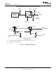
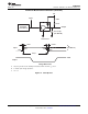
DW OR N PACKAGE
(TOP VIEW)
ULN2803A
www.ti.com
SLRS049G –FEBRUARY 1997–REVISED JANUARY 2015
6 Pin Configuration and Functions
Pin Functions
PIN
TYPE DESCRIPTION
NAME NO.
<1:8>B 1 - 8 I Channel 1 through 7 darlington base input
<1:8>C 18 - 11 O Channel 1 through 7 darlington collector output
GND 7 — Common Emmitter shared by all channels (typically tied to ground)
COM 8 I/O Common cathode node for flyback diodes (required for inductive loads)
Copyright © 1997–2015, Texas Instruments Incorporated Submit Documentation Feedback 3
Product Folder Links: ULN2803A