User's Guide SBOU123 – March 2012 XTR108EVM-USB Evaluation Board and Software Tutorial This user's guide describes the characteristics, operation and use of the XTR108EVM-USB evaluation module (EVM). This EVM is designed to evaluate the performance of the XTR108, an SPI™programmable, current- or voltage-output, two-wire transmitter designed for temperature and bridge sensors. Throughout this document, the terms evaluation board, evaluation module, and EVM are synonymous with the XTR108EVM-USB.
www.ti.com 23 24 25 26 27 28 29 30 31 32 33 34 35 36 37 38 39 40 41 42 ........................................................................................................... XTR108EVM-USB Software, Manual Calibration Tab ................................................................ Adjust RTD Emulator...................................................................................................... Manual Calibration Tab, Post-Calibration ........................................................
www.ti.com 28 XTR108EVM-USB Interface Board Bill of Materials .................................................................. 50 29 XTR108EVM-USB Sensor Board Bill of Materials .................................................................... 51 30 Standard RTD Equations ................................................................................................. 56 31 Mnemonic Commands ....................................................................................................
Overview 1 www.ti.com Overview This document provides the information needed to set up and operate the XTR108EVM-USB evaluation module, which is a test platform for the XTR108 programmable two-wire transmitter and sensor conditioner. For a more detailed description of the XTR108, refer to the product data sheet (SBOS187) available from the Texas Instruments web site at www.ti.com. The XTR108EVM-USB is an evaluation module that is used to fully evaluate the XTR108.
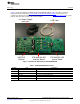
Overview www.ti.com 1.1 XTR108EVM-USB Kit Contents Figure 1 shows the hardware included with the XTR108EVM-USB kit. Table 1 describes each item included in the kit. Contact the Texas Instruments Product Information Center nearest you if any component is missing. It is highly recommended that you also check the XTR108 product folder to verify that you have the latest version of the related software.
Hardware Overview 1.2 www.ti.com Related Documentation from Texas Instruments The documents listed in Table 2 provide information regarding Texas Instruments' hardware used in assembly of the XTR108EVM-USB. This user's guide is available from the TI web site under literature number SBOU123. Any letter appended to the literature number corresponds to the document revision that is current at the time of the writing of this document. Newer revisions may be available from the TI web site at www.ti.
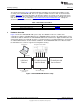
Hardware Overview www.ti.com 2.1 XTR108EVM-USB Theory of Operation Figure 3 shows the block diagram of the XTR108EVM-USB Interface Board and Sensor Board. Digital Multimeter Interface 25-pin DSUB from USB DAQ 5.
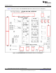
Hardware Overview 2.2 www.ti.com Interface Board Overview Figure 4 shows the location of all XTR108EVM-USB Interface Board connectors and jumpers. Figure 4.
Hardware Overview www.ti.com 2.2.1 Interface Board: Signal Definitions and Pinouts This section provides the signal definitions for all XTR108EVM-USB Interface Board connectors. 2.2.1.1 Multimeter Connect Table 3 shows the signals connected to the Multimeter Connect interface on the Interface Board. Table 3.
Hardware Overview 2.2.1.4 www.ti.com J3 (Io_XTR108) Table 6 shows the signals connected to J3 on the Interface Board. J3 is used to connect the current output of an external XTR108 system to the Interface Board. Table 6. J3 Pinout (Io_XTR108) 2.2.1.5 Pin Name 1 IO+ High-side current output from the XTR108 Description 2 IO– Low-side current output from the XTR108 J4 (Loop Supply) Table 7 shows the signals connected to J4 on the Interface Board. J4 provides the loop power supply to the XTR108.
Hardware Overview www.ti.com 2.2.1.7 J6 (25-Pin Male DSUB) Table 9 shows the signals connected to J6 on the Interface Board. J6 is used to connect the SPI interface and 5.0-V power supply from the USB DAQ to the Interface Board. Table 9. J6 Pinout (25-Pin Male DSUB) 2.2.1.
Hardware Overview 2.2.1.9 www.ti.com J8 (RTD_CON) Table 11 shows the signals connected to J8 on the Interface Board. J8 is used to connect the RTD emulator circuit to an external XTR108 system. Table 11. J8 Pinout (RTD_CON) 2.2.2 Pin Name 1 RCM 2 RZ 3 RTD Description RCM (common-mode resistor) RZ (zero-scale resistor) RTD resistance Interface Board Jumper Settings Table 12 explains the function of the XTR108EVM-USB Interface Board jumpers. Table 12.
Hardware Overview www.ti.com 2.3 Sensor Board Overview Figure 5 shows the location of all XTR108EVM-USB Sensor Board connectors and jumpers. Figure 5.
Hardware Overview 2.3.1 www.ti.com Sensor Board Connections This section provides signal definitions for all XTR108EVM-USB Interface Board connectors. 2.3.1.1 J1 (SPI) Table 13 shows the signals connected to J1 on the Sensor Board. J1 is used to connect an external SPI interface to the Sensor Board. Table 13. J1 Pinout (SPI) 2.3.1.
Hardware Overview www.ti.com 2.3.2 Sensor Board Jumper Settings Table 17 explains the function of the XTR108EVM-USB Interface Board jumpers. Table 17. Sensor Board Jumper Functions Jumper Default JMP1 FET This jumper selects whether to enable or bypass the depletion-mode transistor Q1. Set the jumper to the FET position when using current-output mode. Set the jumper to the BYPASS position when using voltage-output mode.
Hardware Setup 2.3.3 www.ti.com Test Points and Miscellaneous Breadboard Area There are multiple points available on the Sensor Board, including several connections to IRET. IRET is common (labeled as GND on the board) for most XTR108 applications, and is provided for ease of measuring analog signals. Reserved areas with plated-through, standard-spacing, 0.1-inch holes for miscellaneous proof-of-concept breadboarding are also provided on the board.
Hardware Setup www.ti.com 3.2 Connecting the Hardware When first setting up the EVM hardware, It is recommended to first connect the USB DAQ Platform to the XTR108EVM-USB Interface Board. To connect the two PCBs together, gently push on both sides of the 25-pin D-SUB connectors as shown in Figure 7. Make sure that the connectors are completely pushed together because loose connections may cause intermittent operation. Figure 7.
Hardware Setup 3.3 www.ti.com Connecting Power and USB to the USB DAQ Platform After the three XTR108EVM-USB parts are connected, connect the included 6-V power supply (wall-wart) to terminal J5 of the USB DAQ platform. If connected properly, the µC OK, 3.3-V, and VCC LEDs on the USB DAQ illuminate as shown in Figure 9. Always connect power before connecting the USB cable.
Hardware Setup www.ti.com Once power has been applied to the USB DAQ Platform, you can connect one end of the USB cable to the USB DAQ and the other end to a PC USB port, as shown in Figure 10. Figure 11 shows the typical response to connecting the USB DAQ Platform to a PC USB port for the first time. Typically, the computer responds with a Found New Hardware, USB Device pop-up message. The pop-up message typically changes to Found New Hardware, USB Human Interface Device shortly after.
Hardware Setup 3.4 www.ti.com Connecting Loop Power Supply to the XTR108EVM-USB Interface Board Connect a dc lab power supply to J4 on the Interface Board as shown in Figure 12. When operating in current-output mode, the loop-supply input voltage range is 12 V to 24 V. In general, you must consider the power dissipated in the external transistor and the operating temperature of the transistor in order to determine the maximum loop voltage and current.
Hardware Setup www.ti.com 3.5 Connecting Outputs to a Digital Multimeter (DMM) The XTR108EVM-USB contains circuitry that routes the current output, voltage output, and RTD emulator signals to the multimeter connect terminals on the XTR108EVM-USB Interface Board. Any standard lab multimeter that supports dc voltage, dc current, and four-wire resistance measurements is compatible with the XTR108EVM-USB. This EVM is designed and tested with the Agilent 34401A multimeter.
Hardware Setup 3.6 www.ti.com USB DAQ Platform Default Jumper Settings Figure 14 shows the default USB DAQ Platform jumper configuration. In general, these jumpers should not be changed. For more information about the function of these jumpers, refer to the USB DAQ Platform User's Guide. Figure 14.
Hardware Setup www.ti.com 3.7 XTR108EVM-USB Interface Board Default Jumper Settings Figure 15 shows the default XTR108EVM-USB Interface Board jumper configuration. Table 18 summarizes the default jumper configuration. For more information about the jumpers on the Interface Board, see Table 12. Figure 15. XTR108EVM-USB Interface Board Default Jumper Settings Table 18.
Hardware Setup 3.8 www.ti.com XTR108EVM-USB Sensor Board Default Jumper Settings Figure 16 shows the default XTR108EVM-USB Sensor Board jumper configuration. Table 19 summarizes the default jumper configuration. For more information about the jumpers on the Sensor Board, see Table 17. Figure 16.
Software Setup www.ti.com Table 19. XTR108EVM-USB Sensor Board Default Jumper Settings 4 Jumper Position Description JMP1 FET Enable FET sub regulator JMP2 FET Enable FET sub regulator JMP3 IOUT Current-output mode JMP4 NO LOAD JMP5 IOUT JMP6 BYPASS Bypass SPI clock buffer on charge pump JMP7 NO CLK Disable charge pump JMP8 2-WIRE Select two-wire RTD Load resistor disconnected Current-output mode Software Setup This section describes how to install the XTR108EVM-USB software.
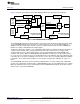
Software Overview 5 www.ti.com Software Overview Once the XTR108EVM-USB starts up, several SPI communications take place to initialize the Interface Board and read the XTR108 register values. Refer to Figure 18 for a screen shot of how the software should appear if the EVM is functioning properly. The actual values of the fields inside the XTR108 block diagram (such as PGA gain or ILIN DAC Linearization) may vary. Figure 18.
Software Overview www.ti.com If there is an error in the communication between the PC and the USB-DAQ, an error message pops up as shown in Figure 19. In this case, it is recommended to close the EVM software, disconnect the power and USB cables from the USB-DAQ, and wait a few moments. Next reconnect the power cable, then reconnect the USB cable. After a few moments, start the XTR108EVM-USB software again. Figure 19. USB Communication Error 5.
Software Overview 5.1.2 www.ti.com PGA The differential input voltage created by the current sources IREF1 and IREF2 flowing through the RTD and RZ resistances is applied to the input pins of a programmable-gain instrumentation amplifier (PGA). The PGA has seven voltage-gain settings in binary steps from 6.25 V/V to 400 V/V. The input common-mode range of the PGA is 0.2 V to 3.5 V above the IRET potential.
Software Overview www.ti.com 5.1.4 I_REF DAC The XTR108 contains two matched, adjustable, reference current sources for sensor excitation. Each current source is controlled by a coarse DAC and fine DAC that together adjust the overall output. The equations that define the output of these current sources are given in Table 22. Note that the external resistor (RSET) is used to convert the DAC reference voltage (VREF) into the reference current.
Software Overview www.ti.com Table 23. Overscale Threshold VO Overscale Threshold IO Overscale Threshold RVI = 6.34 kΩ OS3 OS2 OS1 OS0 0 0 0 0 2.625 V 20.7 mA 0 0 0 1 2.6875 V 21.2 mA 0 0 1 0 2.75 V 21.7 mA 0 0 1 1 2.8125 V 22.2 mA 0 1 0 0 2.875 V 22.7 mA 0 1 0 1 2.9375 V 23.2 mA 0 1 1 0 3.0 V 23.7 mA 0 1 1 1 3.0625 V 24.2 mA 1 0 0 0 3.125 V 24.6 mA 1 0 0 1 3.1875 V 25.1 mA 1 0 1 0 3.25 V 25.6 mA 1 0 1 1 3.3125 V 26.
Software Overview www.ti.com 5.1.7 SPI Interface In normal operation, the XTR108 reads data from an external EEPROM to retrieve calibrated register settings. This operation is accomplished by a read-back controller on the XTR108. The read-back controller defaults to being active when the XTR108 is powered on and is continuously active unless disabled. In other words, it starts a new read operation as soon as the previous operation is completed.
Software Overview 5.2 www.ti.com Find Resistors Tab The Find Resistors tab in the XTR108EVM-USB software allows the user to enter the desired XTR108 operating conditions. Based on the user input, the software calculates the appropriate values for the supporting circuitry and performs error-checking to determine if the desired conditions exceed system capabilities. This tab also allows the user to save a custom configuration as a model file that is used as the basis for calibration.
Software Overview www.ti.com 5.2.1 Step 1: Enter Operating Conditions This area of the Find Resistors tab allows the user to input system operating conditions, including the global system conditions as well as individual conditions for each channel. Global conditions consist of current- or voltage-output mode, output span, and overscale and underscale limiting. Channel-specific conditions include channel enable or disable, temperature span, RTD type, and Callendar-van Dusen (CVD) coefficients. 5.2.1.
Software Overview 5.2.2 www.ti.com Step 2: Calculate Resistor Values When the Calculate Resistors button is clicked, the XTR108EVM-USB software uses the operating conditions entered in Step 1: Enter Operating Commands to calculate the best values for RSET, RLIN, RCM, and RZ (for each enabled channel). The RSET value is critical to proper XTR108 operation (see the I_REF DAC section). If the software cannot find a suitable RSET value, an error message is displayed as shown in Figure 21.
Software Overview www.ti.com 5.2.4 Step 4: Save or Load Model File The XTR108EVM-USB software allows the user to save operating conditions and sensor board resistor values to a model file to facilitate calibration. Click the Save Model File button to open the Save Model File dialog box, as shown in Figure 23. Enter a descriptive file name that contains the output span and some basic configuration information, such as 4-20mA, CH1 0-300C in the image below.
Software Overview 5.3 www.ti.com Manual Calibration Tab The Manual Calibration tab in the XTR108EVM-USB software allows the user to program the XTR108 using a model file, perform a two-point calibration, calculate the post-calibrated error of the system, and calibrate the overscale and underscale output values. Figure 24 shows the Manual Calibration tab with default values. The following sections explain the use of each section of the tab.
Software Overview www.ti.com 5.3.1 Step 1: Initialize Before calibration can take place, a model file must be loaded into the software. The XTR108EVM-USB software automatically loads the most recent model file into memory at startup, but a different model file can be selected by clicking the Load Model File button. The path of the loaded model file is shown in the Model File indicator. After loading a model file, use the channel-to-calibrate control to select which channel should be calibrated.
Software Overview 5.3.3 www.ti.com Step 3: First Corrections Once the initial settings have been written to the XTR108 and the RTD Emulator has been configured, output measurements can be taken at the minimum- and maximum-scale values. Configure the DMM for dc current or dc voltage measurement, depending on which mode is being used. Click the Set RTD Emulator to Minimum Scale button to route the minimum-scale output signal to the DMM.
Software Overview www.ti.com 5.3.7 Verify Calibration After successfully completing the manual calibration procedure, the minimum-scale, mid-scale, and maximum-scale Percent Error indicators should be less than or equal to 0.1%. See Figure 26 for an example of a successful post-calibration screen. Figure 26. Manual Calibration Tab, Post-Calibration 5.3.
Software Overview 5.4 www.ti.com Automatic Calibration Tab The Automatic Calibration tab in the XTR108EVM-USB software allows the user to perform a completely automated calibration of the XTR108 using a previously-saved model file. The entire procedure takes less than a minute to complete and only requires the user to click one button. Figure 27 shows the Automatic Calibration tab. The following sections explain the use of each section of the tab.
Software Overview www.ti.com 5.4.1 DMM Connection At startup, the XTR108EVM-USB software automatically detects if an Agilent 34401A multimeter is connected over the GPIB-to-USB interface. If a 34401A is detected, the DMM Connected? LED turns on, the DMM Status indicator displays the message DMM detected. Proceed with Auto-Cal, and the Initiate Auto-Cal button is enabled. If a 34401A is not detected, the DMM Connected? LED remains off, the DMM Status indicator displays the message DMM not detected.
Software Overview 5.4.6 www.ti.com Verify Calibration If the percentage of minimum-scale, mid-scale, and maximum-scale error after calibration is less than or equal to 0.1%, the Status indicator displays the message Calibration successful! Error < 0.1% and the square status LED turns on (bright green). Figure 28 shows an example of a successful post-calibration screen. If the percentage of error after calibration is greater than 0.1%, the Status indicator displays the message Calibration unsuccessful.
Software Overview www.ti.com 5.5 Registers Tab The Registers tab in the XTR108EVM-USB software enables the user to view and edit the contents of each register internal to the XTR108. Similar to the Block Diagram tab, it is recommended that only advanced users make bit-level changes using this tab. However, for debugging purposes this capability can be extremely useful. Figure 29 shows the Registers tab. The actual values of each register may vary. Figure 29.
Software Overview 5.5.1 www.ti.com Register and EEPROM Communications The six buttons at the top of the Registers tab allow the user to perform read/write operations between the XTR108EVM-USB software and the XTR108 registers and the EEPROM. When clicked, The Read All Reg button reads the current XTR108 register values and loads them into software, overwriting any current values. Similarly, the Write All Reg button writes the current software register values to the actual registers within the XTR108.
Software Overview www.ti.com 5.6 Tools Menu The Tools menu, located in the menu bar in the upper-left corner of the XTR108EVM-USB software, contains additional features useful for debugging or troubleshooting. The following sections explain the use of each option within the Tools menu. 5.6.1 Control Bits The Control Bits window, as shown in Figure 30, enables manual control of the signals that enable and disable the XTR108EVM Interface Board relays.
Software Overview 5.6.2 www.ti.com Debug Window The Debug window, as shown in Figure 31, displays the input and output of all SPI communications. The command lines follow the syntax of the tioScript mnemonic commands. More information on the mnemonic commands is available in the Mnemonic Commands section. Pressing the Clear button clears the strings displayed in the Debug Window until new communications take place. Figure 31. Debug Window 5.6.
General Operating Tips www.ti.com 6 General Operating Tips 6.1 Voltage Output Mode In many applications, it is desirable to bypass the FET and connect the XTR108 directly to the power supply. This configuration can be completed by positioning jumpers JMP2 and JMP3 in the Bypass position. NOTE: You must be careful in this mode to not apply an overvoltage to the XTR108. The XTR108 maximum supply voltage is 5.5 V. The voltage drop across D1 reduces the XTR108 supply voltage by approximately 0.7 V.
Hardware Documentation 7 www.ti.com Hardware Documentation This section provides the hardware documentation for the XTR108EVM-USB, including board schematics, layouts, and bill of materials. 7.1 Schematics Figure 34 shows the XTR108EVM-USB Interface Board schematic. Relay Driver / Control Bits 17 K5 K6 12 K8 1 Relay4 12 12 1 Relay6 12 Relay7 J1 OFF 10 3 9 4 10 OFF 3 10 OFF 3 8 5 3B 3C 4B 4C Relay3 4 9 4 9 4 RTD + 9 ON 5 RTD + 8 TXS2SS-4.
Hardware Documentation www.ti.com Figure 35 shows the XTR108EVM-USB Sensor Board schematic. BBLOGO TI LOGO GND SCK GND GND GND GND GND SDIO VCC SPI_SCK R1 49.9k SPI_DIO CS2 VCC SPI_CS1 C1 0.1uF J1 SDIO 3 SCK 2 CS1 1 8 Vcc 25C040 4 15 18 17 7 3 CS2 Rset SR and Control Circuits OPA OUT RSET 12.1k REFout REFin 21 R9 20 0 Bypass C2 V/I-2 V/I-1 V/I-0 Sub-Reg Driver Vgate Vs 2 14 JMP1 VCC J3 0.01uF 1 Io - Vout VCC Charge Pump 3 JMP5 CP D2 C12 Bypass JMP6 4 2 30.
Hardware Documentation 7.3 www.ti.com Bill of Materials (BOM) Table 28 gives the XTR108EVM-USB Interface Board bill of materials. Table 29 gives the XTR108EVM-USB Sensor Board bill of materials. Table 28. XTR108EVM-USB Interface Board Bill of Materials 50 Qty Value Ref Des 1 10µF C1 Description 3 0.1µF C2-C4 CAP .10UF 16V CERAMIC X7R 0603 8 4.7kΩ R1-R8 RES 4.70K OHM 1/10W 1% 0603 SMD ±100ppm/°C 4 10Ω R9-R12 RES 10.0 OHM 1/10W 0.1% 0603 8 510Ω R13-R20 1 4.
Hardware Documentation www.ti.com Table 29. XTR108EVM-USB Sensor Board Bill of Materials Qty Value Ref Des Vendor Part Number 1 0.1µF C1 CAP CER .10UF 25V X7R 10% 0603 Description TDK Corporation C1608X7R1E104K 1 220pF C8 CAP CER 220PF 50V X7R 10% 0603 TDK Corporation C1608X7R1H221K 1 2.2µF C9 CAP CER 2.
Appendix 8 www.ti.com Appendix This section contains information related to the operation of the XTR108, the equations used during the calibration procedure, and the mnemonic command syntax displayed by the Debug window. 8.1 XTR108 Operation This section describes the operation of key XTR108 functional blocks. 8.1.1 Input MUX The primary function of the XTR108 input multiplexer (MUX) is to allow a single hardware module to function for multiple RTD ranges and types.
Appendix www.ti.com Figure 37 shows the same multiplexer configuration with the RTD at maximum temperature, where TMAX = +850°C. At this point, the differential input voltage to the PGA is equal to 186 mV, the maximum value for this configuration. I1 500PA I2 500PA T=850°C 390.48: 0.718V 500PA 500PA MUX RTD PT100 0.532V RZ2 RZ1 18.7: RZ3 RZ4 RZ5 + PGA Input differential voltage is approximately 186mV at TMAX 1000PA XTR108 RCM 523: VCM = 0.52V Figure 37.
Appendix 8.1.2 www.ti.com RSET The range of the IREF DAC that controls the current sources I1 and I2 is set by the external resistor RSET. For example, with a value of RSET = 12.1 kΩ, the range of IREF is 480 µA to 510 µA. If RSET = 121 kΩ, the range of IREF becomes 48 µA to 51 µA. The Find Resistors tab within the XTR108EVM-USB software helps to determine the appropriate RSET value.
Appendix www.ti.com 8.1.4 Linearity Correction Figure 41 illustrates how the XTR108 linearity correction works. The RTD has a response that is approximately quadratic (gray line). The positive feedback of the input signal through the linearity DAC ILIN generates a response that is also approximately quadratic (black line). The two responses counteract each other to generate a linear output (red line).
Appendix 8.2 www.ti.com XTR108 Calibration Equations (Current-Output Mode) The following section gives the equations used during the calibration procedure for current-output mode. 8.2.1 Initial Calculations 8.2.1.1 RTD Resistance The equations in Table 30 are used to calculate the RTD resistance at the minimum temperature (RTDMIN), medium temperature (RTDMID), and maximum temperature (RTDMAX). Pick an external zero resistor, RZ, that is the closest standard value to RTDMIN. Table 30.
Appendix www.ti.com 8.2.1.5 IZERO DAC (Zero Offset) Calculate the required IZERO DAC value. IZERO = IOUT_MIN - 8.2.1.6 50*APGA*IREF*(RTDMIN - RZ) RVI Calculate DAC Codes The IREF and IZERO DACs are controlled by registers 10, 11, 12, and 13 in the XTR108. Use the following equations to determine the values to be written to these registers. N10, N11, N12, and N13 are decimal values that must be converted to hexadecimal before being written.
Appendix 8.2.2.2 www.ti.com IREF Registers Calculate the corrections for the IREF registers.
Appendix www.ti.com 8.2.3 Second Corrections Measure the output current at the maximum temperature (IOUT_MAX_MEAS_2). 8.2.3.1 Linearization Register Calculate the final corrections for the linearization register. This step completes the calibration procedure. ILIN_A = IREF_B*APGA*50*(RTDMAX-RTDMIN) RVI ILIN_B = IOUT_MAX_MEAS_2 ± IOUT_MIN GLIN_MEAS_A = ILIN_B ± ILIN_A (RTDMAX-RZ_A)*ILIN_B GLIN_FINAL = GLIN_A* GLIN_A GLIN_MEAS_A N14_A = round(16*GLIN_FINAL*RLIN) 8.
Appendix www.ti.com The USB-DAQ Platform SPI protocol supports four clock and data line modes of operation. These modes are summarized in Table 32. The first mode, BREH, is used by the XTR108EVM-USB. Table 32. SPI Modes of Operation Mode Clock Polarity Description (CPOL) Clock Transition for Data Polarity Description (CPHA) BREH Clock idles low CPOL = 0 Data are read by the USB-DAQ on the clock rising edge. Data are changed by the USB-DAQ on the clock falling edge.
FCC Warning This evaluation board/kit is intended for use for ENGINEERING DEVELOPMENT, DEMONSTRATION, OR EVALUATION PURPOSES ONLY and is not considered by TI to be a finished end-product fit for general customer use. It generates, uses, and can radiate radio frequency energy and has not been tested for compliance with the limits of computing devices pursuant to part 15 of FCC rules, which are designed to provide reasonable protection against radio frequency interference.
EVALUATION BOARD/KIT/MODULE (EVM) ADDITIONAL TERMS Texas Instruments (TI) provides the enclosed Evaluation Board/Kit/Module (EVM) under the following conditions: The user assumes all responsibility and liability for proper and safe handling of the goods. Further, the user indemnifies TI from all claims arising from the handling or use of the goods.
FCC Interference Statement for Class B EVM devices This equipment has been tested and found to comply with the limits for a Class B digital device, pursuant to part 15 of the FCC Rules. These limits are designed to provide reasonable protection against harmful interference in a residential installation. This equipment generates, uses and can radiate radio frequency energy and, if not installed and used in accordance with the instructions, may cause harmful interference to radio communications.
【Important Notice for Users of this Product in Japan】 】 This development kit is NOT certified as Confirming to Technical Regulations of Radio Law of Japan If you use this product in Japan, you are required by Radio Law of Japan to follow the instructions below with respect to this product: 1. 2. 3. Use this product in a shielded room or any other test facility as defined in the notification #173 issued by Ministry of Internal Affairs and Communications on March 28, 2006, based on Sub-section 1.
EVALUATION BOARD/KIT/MODULE (EVM) WARNINGS, RESTRICTIONS AND DISCLAIMERS For Feasibility Evaluation Only, in Laboratory/Development Environments. Unless otherwise indicated, this EVM is not a finished electrical equipment and not intended for consumer use.
IMPORTANT NOTICE Texas Instruments Incorporated and its subsidiaries (TI) reserve the right to make corrections, enhancements, improvements and other changes to its semiconductor products and services per JESD46, latest issue, and to discontinue any product or service per JESD48, latest issue. Buyers should obtain the latest relevant information before placing orders and should verify that such information is current and complete.