
User's Manual


3
®
DEM-PCM1717
DEM-PCM1717
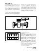
The DEM-PCM1717 is the basic evaluation fixture for the
PCM1717 ∆Σ audio DAC. This fixture provides an easy way
to connect power, data, and interface signals to the DAC.
Figure 1 shows the block diagram of the DEM-PCM1717.
The user must supply 4 digital audio signals, power, and
mode control signals. The DAC will then provide two
channels of either directly or capacitively coupled analog
outputs.
The PCM1717 can be operated either in a hardware or
software mode. In the software mode either external logic or
a processor is used to program four registers internal to the
PCM1717. (Consult the data sheet for additional informa-
tion).
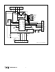
The hardware mode can be evaluated using this fixture by
use of the on board DIP switches. These switches are
connected to pins on the PCM1717 which force either power
or ground to the pin. In the hardware mode some of the
features of the PCM1717 can be exercised. The selection
between the hardware and software mode is done using the
mode switch on the DEM-1717. Figure 2 shows the switch
settings and the resulting functions attained for the PCM1717.
The switches operate in an active low condition.
FIGURE 1. DEM-PCM1717 Block Diagram.
FIGURE 2. DEM-PCM1717 Switch Settings.
HARDWARE DESCRIPTION
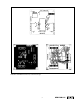
Figure 3 shows the schematic diagram of the DEM-PCM1717
evaluation board.
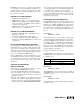
Figure 4 illustrates the PC board design and component
placement for the DEM-PCM1717 evaluation board. Note
on the parts layout that there are 3 connectors CN1, CN2,
and CN3. CN1 is used to connect the digital audio signals to
the PCM1717. CN2 is used connect the control lines for the
PCM1717 as well as power and ground. CN3 is used to
access the audio output from the PCM1717. The analog
outputs are available as DC-coupled (VOR-D, VOL-D) or
ac-coupled (VOR-C, VOL-C). The DC coupled output is
referred to ground, and the AC- coupled output is referred to
V
CC
/2, typically 2.5V. There is also a connection for the
output of the zero detect flag. Use of this pin requires a pull-
up resistor, R
1
. This resistor is labeled R1 on the schematic
and the board and a typical value is 4.7kΩ.
The crystal (U1) is not included.
CN3
CN2
+V
CC
GNDRSTB
MDMCML
+V
CC
R
1
V
O
L • C
V
O
L • D
V
O
R • D
V
O
R • C
ZO
GND
PCM1717E
S1
5
CN1
CLKO
XTI
BCK
LRCK
DIN
GND
4
Mute
On
Mute
Off
Off
48kHz
44.1kHz
32kHz
Off
44.1kHz
DEM-PCM1717
De-Emphasis
48kHz
32kHz
Reset
Off
Reset
On
Hardware
Software
ML MC MD RSTB
Mode
On
Off
Low
High