
User's Manual


LCD Controller Operation
18-4 LCD Controller
18.2 LCD Controller Operation
The LCD controller is configured with user software. The setup and operation
of LCD controller is discussed in the following sections.
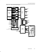
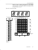
18.2.1 LCD Memory
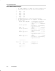
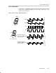
The LCD memory map is shown in Figure 18−2. Each memory bit corresponds
to one LCD segment, or is not used, depending on the mode. To turn on an
LCD segment, its corresponding memory bit is set.
Figure 18−2. LCD memory
--
32103210
Associated
Common Pins
097h
Address
---- ------
------ ------
------ ------
------ ------
------ ------
------ ------
------ ------
------ ------
------ ------
------ ------
------ ------
------ ------
------ ------
------ ------
------ ------
098h
099h
09Ah
09Bh
09Ch
09Dh
09Eh
09Fh
0A0h
0A1h
0A2h
0A3h
0A4h
29, 28
27, 26
25, 24
23, 22
21, 20
19, 18
17, 16
15, 14
13, 12
11, 10
9, 8
7, 6
5, 4
3, 2
1, 0
7
0
--
--
--
--
--
--
--
--
--
--
--
--
--
--
--
--
--
--
--
--
--
--
--
--
--
--
--
--
--
--
Associated
Segment Pins
Sn+1
Sn
28
26
24
22
20
18
16
14
12
10
8
6
4
2
0
n
------ ------
------ ------
------ ------
------ ------
------ ------
--
--
--
--
--
--
--
--
--
--
092h
093h
094h
095h
096h
31, 30
33, 32
35, 34
37, 36
39, 38
30
32
34
36
38
091h
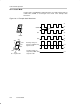
18.2.2 Blinking the LCD
The LCD controller supports blinking. The LCDSON bit is ANDed with each
segment’s memory bit. When LCDSON = 1, each segment is on or off
according to its bit value. When LCDSON = 0, each LCD segment is off.
18.2.3 LCD Timing Generation
The LCD controller uses the f
LCD
signal from the Basic Timer1 to generate the
timing for common and segment lines. The proper frequency f
LCD
depends on
the LCD’s requirement for framing frequency and LCD multiplex rate. See the
Basic Timer1 chapter for more information on configuring the f
LCD
frequency.