
User's Manual

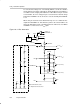

LCD_A Controller Introduction
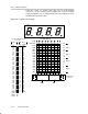
19-3LCD_A Controller
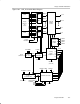
Figure 19−1. LCD_A Controller Block Diagram
VLCDREFx
Display
Memory
20x
8−bits
Segment
Output
Control
Mux
Analog
Voltage
Multiplexer
Timing
Generator
COM0
COM2
COM1
COM3
S0
S1
Common
Output
Control
S39
S38
SEG0
SEG1
SEG38
SEG39
Mux
Mux
Mux
LCDSx
LCDMXx
LCDSON
LCDON
f
LCD
OSCOFF
(from SR)
V1
V2
V3
V4
VDVCVBVA
091h
0A4h
ACLK
32768 Hz
LCDFREQx
Regulated Charge
Pump/
Contrast Control
VLCDx
V
LCD
LCDCAP/R33
LCD Bias Generator
V1
V
LCD
LCD2B
LCDMXx
V2
V3
V4
LCDCPEN
V5
V5
Divider
/32 .. /512
4
REXT
R23
LCDREF/
R13
R03
R03EXT
10