
User's Manual


System Implementation
1-8
1.2 System Implementation
This section describes signal connection for each interface, PCI bus, PC card
interface, I
2
C interface, P
2
C interface, ZV interface, interrupt interface (parallel
and serial), miscellaneous signals, and the PHY-Link interface. It also explains
pullup/pulldown resistor requirements.
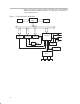
1.2.1 Clamping Rails
The PCI445X device has three clamping rails: V
CCA
, V
CCB
, and V
CCP
. V
CCA
and V
CCB
are not power supplies for PC cards. After a card is powered up, the
supply voltage to the card is fed back into the V
CCA
(or V
CCB
) input to the
controller. This provides the controller a clamping level for signals to the card.
Technically the power switch controlling V
CCA
is also supplying power to the
card via this signal, but actually V
CCA
is not a signal via which the controller
supplies power to the card.
The PCI445X device only drives out a maximum signal of 3.3 V due to the
3.3-V core. This is not a problem, as 3.3 V is still seen as a logic 1 to a 5-V
system.
V
CCA
and V
CCB
PC Card interface clamping rails. CD1, CD2, VS1, VS2, and STSCHG/RI
are not clamped, because these terminals should be able to signal without
V
CCA
/V
CCB
.
V
CCP
PCI bus interface clamping rail. It includes the MFUNC7/LOCK,
MFUNC7–MFUNC0, IRQSER, GRST, and P
2
C terminals. It excludes
INTA, INTB, INTC, and PME.
Note:
The PME/RI_OUT terminal uses an open drain (OD) buffer.
1.2.2 PCI Bus Interface
PCLK, AD31–AD0, C/BE3–C/BE0, PAR, DEVSEL, FRAME, STOP,
TRDY, IRDY, GNT, REQ
These terminals can be connected to the system PCI bus directly. GNT
and REQ are dedicated signals from the PCI bus arbitrator.
PERR, SERR, and LOCK
PERR and SERR are required signals. LOCK is an optional signal and
available in MFUNC1, MFUNC3, and MFUNC7.
IDSEL
If there is a pulldown on LATCH, then the IDSEL will be routed to AD23, but
the consequence of this is that the system designer must use AD23 as