TMS320C6454 Fixed-Point Digital Signal Processor www.ti.com SPRS311A – APRIL 2006 – REVISED DECEMBER 2006 1 TMS320C6454 Fixed-Point Digital Signal Processor • • • • • High-Performance Fixed-Point DSP (C6454) – 1.39-, 1.
TMS320C6454 Fixed-Point Digital Signal Processor www.ti.com SPRS311A – APRIL 2006 – REVISED DECEMBER 2006 1.1.1 ZTZ/GTZ BGA Package (Bottom View) The TMS320C6454 devices are designed for a package temperature range of 0°C to +90°C (commercial temperature range).
www.ti.com TMS320C6454 Fixed-Point Digital Signal Processor SPRS311A – APRIL 2006 – REVISED DECEMBER 2006 The C64x+ DSP core employs eight functional units, two register files, and two data paths. Like the earlier C6000 devices, two of these eight functional units are multipliers or .M units. Each C64x+ .M unit doubles the multiply throughput versus the C64x core by performing four 16-bit x 16-bit multiply-accumulates (MACs) every clock cycle.
TMS320C6454 Fixed-Point Digital Signal Processor www.ti.com SPRS311A – APRIL 2006 – REVISED DECEMBER 2006 1.3 Functional Block Diagram Figure 1-2 shows the functional block diagram of the C6454 device.
TMS320C6454 Fixed-Point Digital Signal Processor www.ti.com SPRS311A – APRIL 2006 – REVISED DECEMBER 2006 Contents TMS320C6454 Fixed-Point Digital Signal Processor.................................................. 1 1.1 Features .............................................. 1 1.1.1 ZTZ/GTZ BGA Package (Bottom View) .............. 2 2 3 4 5 1.2 Description ............................................ 2 1.3 Functional Block Diagram ............................ 4 6 Device Overview .............
TMS320C6454 Fixed-Point Digital Signal Processor www.ti.com SPRS311A – APRIL 2006 – REVISED DECEMBER 2006 2 Device Overview 2.1 Device Characteristics Table 2-1, provides an overview of the C6454 DSP. The tables show significant features of the C6454 device, including the capacity of on-chip RAM, the peripherals, the CPU frequency, and the package type with pin count. Table 2-1.
TMS320C6454 Fixed-Point Digital Signal Processor www.ti.com SPRS311A – APRIL 2006 – REVISED DECEMBER 2006 Table 2-1. Characteristics of the C6454 Processor (continued) HARDWARE FEATURES Device Part Numbers (For more details on the C64x+™ DSP part numbering, see Figure 2-12) C6454 TMX320C6454ZTZ7, TMX320C6454ZTZ8, TMX320C6454ZTZ 2.2 CPU (DSP Core) Description The C64x+ Central Processing Unit (CPU) consists of eight functional units, two register files, and two data paths as shown in Figure 2-1.
TMS320C6454 Fixed-Point Digital Signal Processor www.ti.com SPRS311A – APRIL 2006 – REVISED DECEMBER 2006 Other new features include: • SPLOOP - A small instruction buffer in the CPU that aids in creation of software pipelining loops where multiple iterations of a loop are executed in parallel. The SPLOOP buffer reduces the code size associated with software pipelining. Furthermore, loops in the SPLOOP buffer are fully interruptible.
TMS320C6454 Fixed-Point Digital Signal Processor www.ti.com ÁÁ ÁÁ ÁÁ Á ÁÁ Á ÁÁ Á Á Á Á Á Á Á Á Á Á Á Á Á Á Á Á Á Á Á Á Á Á Á Á Á Á Á Á Á Á Á Á Á SPRS311A – APRIL 2006 – REVISED DECEMBER 2006 src1 Odd register file A (A1, A3, A5...A31) src2 .L1 odd dst Even register file A (A0, A2, A4...A30) (D) even dst long src ST1b ST1a 32 MSB 32 LSB long src Data path A .S1 8 8 even dst odd dst src1 (D) src2 LD1a src2 32 MSB 32 LSB DA1 DA2 LD2a LD2b Á Á Á Á Á Á 32 32 (A) (B) (C) dst .
TMS320C6454 Fixed-Point Digital Signal Processor www.ti.com SPRS311A – APRIL 2006 – REVISED DECEMBER 2006 2.3 Memory Map Summary Table 2-2 shows the memory map address ranges of the C6454 device. The external memory configuration register address ranges in the C6454 device begin at the hex address location 0x7000 0000 for EMIFA and hex address location 0x7800 0000 for DDR2 Memory Controller. Table 2-2.
TMS320C6454 Fixed-Point Digital Signal Processor www.ti.
TMS320C6454 Fixed-Point Digital Signal Processor www.ti.com SPRS311A – APRIL 2006 – REVISED DECEMBER 2006 2.4 Boot Sequence The boot sequence is a process by which the DSP's internal memory is loaded with program and data sections and the DSP's internal registers are programmed with predetermined values. The boot sequence is started automatically after each power-on reset, warm reset, and system reset. For more details on the initiators of these resets, see Section 7.6, Reset Controller.
www.ti.com TMS320C6454 Fixed-Point Digital Signal Processor • • • 2.4.2 such as Code Composer Studio. For the PCI host boot, the CPU is out of reset, but it executes an IDLE instruction until a DSP interrupt is generated by the host. The host can generate a DSP interrupt through the PCI peripheral by setting the DSPINT bit in the Back-End Application Interrupt Enable Set Register (PCIBINTSET) and the Status Set Register (PCISTATSET).
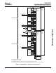
TMS320C6454 Fixed-Point Digital Signal Processor www.ti.com SPRS311A – APRIL 2006 – REVISED DECEMBER 2006 2.5 Pin Assignments 2.5.1 Pin Map Figure 2-2 through Figure 2-5 show the C6454 pin assigments in four quadrants (A, B, C, and D).
TMS320C6454 Fixed-Point Digital Signal Processor www.ti.
TMS320C6454 Fixed-Point Digital Signal Processor www.ti.
TMS320C6454 Fixed-Point Digital Signal Processor www.ti.
TMS320C6454 Fixed-Point Digital Signal Processor www.ti.com SPRS311A – APRIL 2006 – REVISED DECEMBER 2006 2.6 Signal Groups Description CLKIN1 SYSCLK4/GP[1] (A) PLLV1 Clock/PLL1 and PLL Controller Reset and Interrupts RESETSTAT RESET NMI POR CLKIN2 PLLV2 Clock/PLL2 RSV02 RSV03 RSV04 RSV05 RSV06 RSV07 TMS TDO TDI TCK TRST PRODUCT PREVIEW Reserved EMU0 EMU1 • • • EMU14 EMU15 EMU16 EMU17 EMU18 IEEE Standard 1149.
TMS320C6454 Fixed-Point Digital Signal Processor www.ti.com SPRS311A – APRIL 2006 – REVISED DECEMBER 2006 TINPL1 Timer 1 Timer 0 TOUTL1 TOUTL0 TINPL0 Timers (64-Bit) PREQ/GP[15](C) PINTA/GP[14](C) PRST/GP[13](C) PGNT/GP[12](C) FSX1/GP[11](B) FSR1/GP[10](B) DX1/GP[9](B) DR1/GP[8](B) GPIO GP[7] GP[6] GP[5] GP[4] CLKX1/GP[3](B) PCBE0/GP[2](C) SYSCLK4/GP[1](A) CLKR1/GP[0](B) General-Purpose Input/Output 0 (GPIO) Port This pin functions as GP[1] by default.
TMS320C6454 Fixed-Point Digital Signal Processor www.ti.
TMS320C6454 Fixed-Point Digital Signal Processor www.ti.com SPRS311A – APRIL 2006 – REVISED DECEMBER 2006 HCNTL0/PSTOP HCNTL1/PDEVSEL HPI(A) (Host-Port Interface) Data HAS/PPAR HR/W/PCBE2 HCS/PPERR HDS1/PSERR HDS2/PCBE1 HRDY/PIRDY HINT/PFRAME Register Select Control HHWIL/PCLK (HPI16 ONLY) Half-Word Select McBSP1 McBSP0 CLKX1/GP[3] FSX1/GP[11] DX1/GP[9] Transmit Transmit CLKR1/GP[0] FSR1/GP[10] DR1/GP[8] Receive Receive Clock McBSPs (Multichannel Buffered Serial Ports)(B) I2C A. B.
TMS320C6454 Fixed-Point Digital Signal Processor www.ti.
TMS320C6454 Fixed-Point Digital Signal Processor www.ti.com SPRS311A – APRIL 2006 – REVISED DECEMBER 2006 32 HD[15:0]/AD[15:0] HD[31:16]/AD[31:16] PCBE3 HR/W/PCBE2 HDS2/PCBE1 PCBE0/GP[2] PGNT/GP[12] Data/Address Command Byte Enable Clock Control Arbitration Error PREQ/GP[15] HHWIL/PCLK PIDSEL HCNTL1/PDEVSEL HINT/PFRAME PINTA/GP[14] HAS/PPAR PRST/GP[13] HRDY/PIRDY HCNTL0/PSTOP PTRDY HDS1/PSERR HCS/PPERR PCI Interface(A) These PCI pins are muxed with the HPI or GPIO peripherals.
TMS320C6454 Fixed-Point Digital Signal Processor www.ti.com SPRS311A – APRIL 2006 – REVISED DECEMBER 2006 2.7 Terminal Functions The terminal functions table (Table 2-3) identifies the external signal names, the associated pin (ball) numbers along with the mechanical package designator, the pin type (I, O/Z, or I/O/Z), whether the pin has any internal pullup/pulldown resistors, and a functional pin description.
TMS320C6454 Fixed-Point Digital Signal Processor www.ti.com SPRS311A – APRIL 2006 – REVISED DECEMBER 2006 Table 2-3. Terminal Functions (continued) NO. TYPE (1) IPD/IPU (2) DESCRIPTION IPD Nonmaskable interrupt, edge-driven (rising edge) Any noise on the NMI pin may trigger an NMI interrupt; therefore, if the NMI pin is not used, it is recommended that the NMI pin be grounded versus relying on the IPD.
TMS320C6454 Fixed-Point Digital Signal Processor www.ti.com SPRS311A – APRIL 2006 – REVISED DECEMBER 2006 Table 2-3. Terminal Functions (continued) SIGNAL NAME PTRDY HD31/AD31 NO. P4 TYPE (1) IPD/IPU (2) DESCRIPTION PRODUCT PREVIEW I/O/Z PCI target ready (PRTDY) (I/O/Z). By default, this pin has no function.
TMS320C6454 Fixed-Point Digital Signal Processor www.ti.com SPRS311A – APRIL 2006 – REVISED DECEMBER 2006 Table 2-3. Terminal Functions (continued) SIGNAL NAME NO.
TMS320C6454 Fixed-Point Digital Signal Processor www.ti.com SPRS311A – APRIL 2006 – REVISED DECEMBER 2006 Table 2-3. Terminal Functions (continued) SIGNAL NAME NO.
TMS320C6454 Fixed-Point Digital Signal Processor www.ti.com SPRS311A – APRIL 2006 – REVISED DECEMBER 2006 Table 2-3. Terminal Functions (continued) NO.
TMS320C6454 Fixed-Point Digital Signal Processor www.ti.com SPRS311A – APRIL 2006 – REVISED DECEMBER 2006 Table 2-3. Terminal Functions (continued) SIGNAL NAME NO.
TMS320C6454 Fixed-Point Digital Signal Processor www.ti.com SPRS311A – APRIL 2006 – REVISED DECEMBER 2006 Table 2-3. Terminal Functions (continued) SIGNAL AED21 NO.
TMS320C6454 Fixed-Point Digital Signal Processor www.ti.com SPRS311A – APRIL 2006 – REVISED DECEMBER 2006 Table 2-3. Terminal Functions (continued) SIGNAL NAME NO. TYPE (1) IPD/IPU (2) DESCRIPTION DSDDQS3 E23 I/O/Z DSDDQS2 E20 I/O/Z DSDDQS1 E8 I/O/Z DSDDQS0 E11 I/O/Z DSDDQS3 D23 I/O/Z DSDDQS2 D20 I/O/Z DDR2 data strobe [3:0] negative DSDDQS1 D8 I/O/Z Note: These pins are used to meet AC timings.
TMS320C6454 Fixed-Point Digital Signal Processor www.ti.com SPRS311A – APRIL 2006 – REVISED DECEMBER 2006 Table 2-3. Terminal Functions (continued) SIGNAL NAME NO.
TMS320C6454 Fixed-Point Digital Signal Processor www.ti.com SPRS311A – APRIL 2006 – REVISED DECEMBER 2006 Table 2-3. Terminal Functions (continued) SIGNAL NAME NO.
TMS320C6454 Fixed-Point Digital Signal Processor www.ti.com SPRS311A – APRIL 2006 – REVISED DECEMBER 2006 Table 2-3. Terminal Functions (continued) SIGNAL NAME NO. TYPE (1) IPD/IPU (2) DESCRIPTION MCOL K3 I/O/Z This pin is the EMAC collision sense (MCDL) (I) for MII [default] or GMII. MACSEL[1:0] dependent. MTXEN/RMTXEN J5 I/O/Z This pin is either the EMAC transmit enable (MTXEN) (O) for MII [default], RMII, or GMII. MACSEL[1:0] dependent.
TMS320C6454 Fixed-Point Digital Signal Processor www.ti.com SPRS311A – APRIL 2006 – REVISED DECEMBER 2006 Table 2-3. Terminal Functions (continued) SIGNAL NAME NO. TYPE (1) IPD/IPU (2) DESCRIPTION C24 Reserved. This pin must be connected to the 1.8-V I/O supply (DVDD18) via a 200-Ω resistor for proper device operation. NOTE: If the DDR2 Memory Controller is not used, the VREFSSTL, RSV11, and RSV12 pins can be connected directly to ground (VSS) to save power.
TMS320C6454 Fixed-Point Digital Signal Processor www.ti.com SPRS311A – APRIL 2006 – REVISED DECEMBER 2006 Table 2-3. Terminal Functions (continued) NO.
TMS320C6454 Fixed-Point Digital Signal Processor www.ti.com SPRS311A – APRIL 2006 – REVISED DECEMBER 2006 Table 2-3. Terminal Functions (continued) SIGNAL NAME NO. TYPE (1) IPD/IPU (2) DESCRIPTION PRODUCT PREVIEW RSV34 E6 Reserved. This pin must be connected to the 1.8-V I/O supply (DVDD18) via a 1-kΩ resistor for proper device operation. RSV35 D6 Reserved. This pin must be connected directly to ground for proper device operation.
TMS320C6454 Fixed-Point Digital Signal Processor www.ti.com SPRS311A – APRIL 2006 – REVISED DECEMBER 2006 Table 2-3. Terminal Functions (continued) SIGNAL NAME NO. VREFHSTL B2 AVDLL1 A13 AVDLL2 E18 TYPE (1) IPD/IPU (2) DESCRIPTION A (DVDD15/2)-V reference for HSTL buffer (EMAC RGMII). VREFHSTL can be generated directly from DVDD15 using two 1-kΩ resistors to form a resistor divider circuit.
TMS320C6454 Fixed-Point Digital Signal Processor www.ti.com SPRS311A – APRIL 2006 – REVISED DECEMBER 2006 Table 2-3. Terminal Functions (continued) SIGNAL NAME NO. TYPE (1) IPD/IPU (2) DESCRIPTION A29 E26 E28 G2 H23 H28 J6 J24 K1 K7 K23 L24 M7 M23 M28 PRODUCT PREVIEW N24 P6 P28 R1 R6 R23 DVDD33 T7 S 3.
TMS320C6454 Fixed-Point Digital Signal Processor www.ti.com SPRS311A – APRIL 2006 – REVISED DECEMBER 2006 Table 2-3. Terminal Functions (continued) SIGNAL NAME NO. TYPE (1) IPD/IPU (2) DESCRIPTION AD5 AD7 AD14 AD18 AD22 AD24 AE6 AE8 AE15 AF1 AF16 DVDD33 AF24 S 3.3-V I/O supply voltage S 1.
TMS320C6454 Fixed-Point Digital Signal Processor www.ti.com SPRS311A – APRIL 2006 – REVISED DECEMBER 2006 Table 2-3. Terminal Functions (continued) SIGNAL NAME NO. TYPE (1) IPD/IPU (2) DESCRIPTION R18 T11 T13 T15 T17 T19 U12 CVDD U14 S 1.
TMS320C6454 Fixed-Point Digital Signal Processor www.ti.com SPRS311A – APRIL 2006 – REVISED DECEMBER 2006 Table 2-3. Terminal Functions (continued) SIGNAL NAME NO.
TMS320C6454 Fixed-Point Digital Signal Processor www.ti.com SPRS311A – APRIL 2006 – REVISED DECEMBER 2006 Table 2-3. Terminal Functions (continued) SIGNAL NAME NO.
TMS320C6454 Fixed-Point Digital Signal Processor www.ti.com SPRS311A – APRIL 2006 – REVISED DECEMBER 2006 Table 2-3. Terminal Functions (continued) SIGNAL NAME NO.
TMS320C6454 Fixed-Point Digital Signal Processor www.ti.com SPRS311A – APRIL 2006 – REVISED DECEMBER 2006 Table 2-3. Terminal Functions (continued) SIGNAL NAME NO.
TMS320C6454 Fixed-Point Digital Signal Processor www.ti.com SPRS311A – APRIL 2006 – REVISED DECEMBER 2006 2.8 Development 2.8.1 Development Support In case the customer would like to develop their own features and software on the C6454 device, TI offers an extensive line of development tools for the TMS320C6000™ DSP platform, including tools to evaluate the performance of the processors, generate code, develop algorithm implementations, and fully integrate and debug software and hardware modules.
TMS320C6454 Fixed-Point Digital Signal Processor www.ti.com SPRS311A – APRIL 2006 – REVISED DECEMBER 2006 TI device nomenclature also includes a suffix with the device family name. This suffix indicates the package type (for example, ZTZ), the temperature range (for example, blank is the default commercial temperature range), and the device speed range, in megahertz (for example, blank is 1000 MHz [1 GHz]).
TMS320C6454 Fixed-Point Digital Signal Processor www.ti.com SPRS311A – APRIL 2006 – REVISED DECEMBER 2006 SPRU889 High-Speed DSP Systems Design Reference Guide. Provides recommendations for meeting the many challenges of high-speed DSP system design. These recommendations include information about DSP audio, video, and communications systems for the C5000 and C6000 DSP platforms. SPRU970 TMS320C645x DSP DDR2 Memory Controller User's Guide.
TMS320C6454 Fixed-Point Digital Signal Processor www.ti.com SPRS311A – APRIL 2006 – REVISED DECEMBER 2006 3 Device Configuration On the C6454 device, certain device configurations like boot mode, pin multiplexing, and endianess, are selected at device reset. The status of the peripherals (enabled/disabled) is determined after device reset. By default, the peripherals on the C6454 device are disabled and need to be enabled by software before being used. 3.
TMS320C6454 Fixed-Point Digital Signal Processor www.ti.com SPRS311A – APRIL 2006 – REVISED DECEMBER 2006 Table 3-1. C6454 Device Configuration Pins (AEA[19:0], ABA[1:0], and PCI_EN) (continued) CONFIGURATION PIN NO. IPD/ IPU (1) FUNCTIONAL DESCRIPTION HPI peripheral bus width select (HPI_WIDTH). AEA14 R25 0 HPI operates in HPI16 mode (default). HPI bus is 16 bits wide; HD[15:0] pins are used and the remaining HD[31:16] pins are reserved pins in the Hi-Z state. 1 HPI operates in HPI32 mode.
TMS320C6454 Fixed-Point Digital Signal Processor www.ti.com SPRS311A – APRIL 2006 – REVISED DECEMBER 2006 Table 3-1. C6454 Device Configuration Pins (AEA[19:0], ABA[1:0], and PCI_EN) (continued) CONFIGURATION PIN NO. IPD/ IPU (1) FUNCTIONAL DESCRIPTION PCI pin function enable bit (PCI_EN). Selects which function is enabled on the HPI/PCI multiplexed pins. PCI_EN Y29 IPD 0 HPI pin function enabled (default) This means all multiplexed HPI/PCI pins function as HPI pins.
TMS320C6454 Fixed-Point Digital Signal Processor www.ti.com SPRS311A – APRIL 2006 – REVISED DECEMBER 2006 Table 3-2.
TMS320C6454 Fixed-Point Digital Signal Processor www.ti.com SPRS311A – APRIL 2006 – REVISED DECEMBER 2006 Following device reset, all peripherals that are not in the static powerdown state are in the disabled state by default. Peripherals used for boot such as HPI and PCI are enabled automatically following a device reset. Peripherals are only allowed certain transitions between states (see Figure 3-1). Static Powerdown Reset Enable In Progress Disabled Enabled PRODUCT PREVIEW Figure 3-1.
TMS320C6454 Fixed-Point Digital Signal Processor www.ti.com SPRS311A – APRIL 2006 – REVISED DECEMBER 2006 3.4 Device State Control Registers The C6454 device has a set of registers that are used to control the status of its peripherals. These registers are shown in Table 3-5 and described in the next sections. NOTE The device state control registers can only be accessed using the CPU or the emulator. Table 3-5.
TMS320C6454 Fixed-Point Digital Signal Processor www.ti.com SPRS311A – APRIL 2006 – REVISED DECEMBER 2006 3.4.1 Peripheral Lock Register Description When written with correct 32-bit key (0x0F0A0B00), the Peripheral Lock Register (PERLOCK) allows one write to the PERCFG0 register within 16 SYSCLK3 cycles. NOTE The instructions that write to the PERLOCK and PERCFG0 registers must be in the same fetch packet if code is being executed from external memory.
TMS320C6454 Fixed-Point Digital Signal Processor www.ti.com SPRS311A – APRIL 2006 – REVISED DECEMBER 2006 3.4.2 Peripheral Configuration Register 0 Description The Peripheral Configuration Register (PERCFG0) is used to change the state of the peripherals. One write is allowed to this register within 16 SYSCLK3 cycles after the correct key is written to the PERLOCK register.
TMS320C6454 Fixed-Point Digital Signal Processor www.ti.com SPRS311A – APRIL 2006 – REVISED DECEMBER 2006 Table 3-7. Peripheral Configuration Register 0 (PERCFG0) Field Descriptions (continued) Bit Field 12 I2CCTL Description Mode control for I2C 0 Set I2C to disabled mode 1 Set I2C to enabled mode 11 Reserved Reserved. 10 GPIOCTL Mode control for GPIO 0 Set GPIO to disabled mode 1 Set GPIO to enabled mode 9 Reserved Reserved.
TMS320C6454 Fixed-Point Digital Signal Processor www.ti.com SPRS311A – APRIL 2006 – REVISED DECEMBER 2006 3.4.3 Peripheral Configuration Register 1 Description The Peripheral Configuration Register (PERCFG1) is used to enable the EMIFA and DDR2 Memory Controller. EMIFA and the DDR2 Memory Controller do not have corresponding status bits in the Peripheral Status Registers. The EMIFA and DDR2 Memory Controller peripherals can be used within 16 SYSCLK3 cycles after EMIFACTL and DDR2CTL are set to 1.
TMS320C6454 Fixed-Point Digital Signal Processor www.ti.com SPRS311A – APRIL 2006 – REVISED DECEMBER 2006 3.4.4 Peripheral Status Registers Description The Peripheral Status Registers (PERSTAT0 and PERSTAT1) show the status of the C6454 peripherals.
TMS320C6454 Fixed-Point Digital Signal Processor www.ti.com SPRS311A – APRIL 2006 – REVISED DECEMBER 2006 Table 3-9.
TMS320C6454 Fixed-Point Digital Signal Processor www.ti.com SPRS311A – APRIL 2006 – REVISED DECEMBER 2006 31 16 Reserved R-0 15 3 2 0 Reserved PCISTAT R-0 R-0 LEGEND: R = Read only; -n = value after reset Figure 3-7. Peripheral Status Register 1 (PERSTAT1) - 0x02AC 0018 Table 3-10.
TMS320C6454 Fixed-Point Digital Signal Processor www.ti.com SPRS311A – APRIL 2006 – REVISED DECEMBER 2006 3.4.5 EMAC Configuration Register (EMACCFG) Description The EMAC Configuration Register (EMACCFG) is used to assert and deassert the reset of the Reduced Media Independent Interface (RMII) logic of the EMAC. For more details on how to use this register, see Section 7.14, Ethernet MAC (EMAC).
TMS320C6454 Fixed-Point Digital Signal Processor www.ti.com SPRS311A – APRIL 2006 – REVISED DECEMBER 2006 3.4.6 Emulator Buffer Powerdown Register (EMUBUFPD) Description The Emulator Buffer Powerdown Register (EMUBUFPD) is used to control the state of the pin buffers of emulator pins EMU[18:2]. These buffers can be powered down if the device trace feature is not needed. 31 8 Reserved R-0 7 Reserved 1 0 EMUCTL R-0 R/W-0 LEGEND: R/W = Read/Write; R = Read only; -n = value after reset Figure 3-9.
TMS320C6454 Fixed-Point Digital Signal Processor www.ti.com SPRS311A – APRIL 2006 – REVISED DECEMBER 2006 3.5 Device Status Register Description The device status register depicts the device configuration selected upon device reset. Once set, these bits will remain set until a device reset. For the actual register bit names and their associated bit field descriptions, see Figure 3-10 and Table 3-13.
TMS320C6454 Fixed-Point Digital Signal Processor www.ti.com SPRS311A – APRIL 2006 – REVISED DECEMBER 2006 Table 3-13. Device Status Register (DEVSTAT) Field Descriptions (continued) Bit Field 14 MCBSP1_EN 13 Description McBSP1 Enable (MCBSP1_EN) status bit Shows the status of which function is enabled on the McBSP1/GPIO muxed pins.
TMS320C6454 Fixed-Point Digital Signal Processor www.ti.com SPRS311A – APRIL 2006 – REVISED DECEMBER 2006 Table 3-13. Device Status Register (DEVSTAT) Field Descriptions (continued) Bit Field 3:0 BOOTMODE[3:0] Value Description Boot mode configuration bits Shows the status of what device boot mode configuration is operational. BOOTMODE[3:0] [Note: if selected for boot, the corresponding peripheral is automatically enabled after device reset.
TMS320C6454 Fixed-Point Digital Signal Processor www.ti.com SPRS311A – APRIL 2006 – REVISED DECEMBER 2006 • Other Input Pins: If the IPU/IPD does not match the desired value/state, use an external pullup/pulldown resistor to pull the signal to the opposite rail. For the device configuration pins (listed in Table 3-1), if they are both routed out and 3-stated (not driven), it is strongly recommended that an external pullup/pulldown resistor be implemented.
TMS320C6454 Fixed-Point Digital Signal Processor www.ti.com SPRS311A – APRIL 2006 – REVISED DECEMBER 2006 3.8 Configuration Examples Figure 3-12 and Figure 3-13 illustrate examples of peripheral selections/options that are configurable on the C6454 device.
TMS320C6454 Fixed-Point Digital Signal Processor www.ti.
www.ti.com TMS320C6454 Fixed-Point Digital Signal Processor SPRS311A – APRIL 2006 – REVISED DECEMBER 2006 4 System Interconnect On the C6454 device, the C64x+ Megamodule, the EDMA3 transfer controllers, and the system peripherals are interconnected through two switch fabrics. The switch fabrics allow for low-latency, concurrent data transfers between master peripherals and slave peripherals.
TMS320C6454 Fixed-Point Digital Signal Processor www.ti.com SPRS311A – APRIL 2006 – REVISED DECEMBER 2006 4.2 Data Switch Fabric Connections Figure 4-1 shows the connection between slaves and masters through the data switched central resource (SCR). Masters are shown on the right and slaves on the left. The data SCR connects masters to slaves via 128-bit data buses running at a SYSCLK2 frequency.
TMS320C6454 Fixed-Point Digital Signal Processor www.ti.
TMS320C6454 Fixed-Point Digital Signal Processor www.ti.com SPRS311A – APRIL 2006 – REVISED DECEMBER 2006 Table 4-1. SCR Connection Matrix McBSPs CONFIGURATION SCR PCI DDR2 MEMORY CONTROLLER EMIFA MEGAMODULE TC0 N N N Y Y Y TC1 Y Y Y Y Y Y TC2 N N Y Y Y Y TC3 N N Y Y Y Y EMAC N N N Y Y Y HPI N Y N Y Y Y PCI N Y N Y Y Y 4.
TMS320C6454 Fixed-Point Digital Signal Processor www.ti.
TMS320C6454 Fixed-Point Digital Signal Processor www.ti.com SPRS311A – APRIL 2006 – REVISED DECEMBER 2006 4.4 Priority Allocation On the C6454 device, each of the masters (excluding the C64x+ Megamodule) are assigned a priority via the Priority Allocation Register (PRI_ALLOC), see Figure 4-3. The priority is enforced when several masters in the system are vying for the same endpoint. A value of 000b has the highest priority, while 111b has the lowest priority.
TMS320C6454 Fixed-Point Digital Signal Processor www.ti.com SPRS311A – APRIL 2006 – REVISED DECEMBER 2006 5 C64x+ Megamodule The C64x+ Megamodule consists of several components — the C64x+ CPU, the L1 program and data memory controllers, the L2 memory controller, the internal DMA (IDMA), the interrupt controller, power-down controller, and external memory controller.
TMS320C6454 Fixed-Point Digital Signal Processor www.ti.com SPRS311A – APRIL 2006 – REVISED DECEMBER 2006 • Region 1 size is 32K bytes with no wait states. L1D is a two-way set-associative cache while L1P is a direct-mapped cache. The L1P and L1D cache can be reconfigured via software through the L1PMODE field of the L1P Configuration Register (L1PMODE) and the L1DMODE field of the L1D Configuration Register (L1DCFG) of the C64x+ Megamodule.
TMS320C6454 Fixed-Point Digital Signal Processor www.ti.
TMS320C6454 Fixed-Point Digital Signal Processor www.ti.com SPRS311A – APRIL 2006 – REVISED DECEMBER 2006 5.2 Memory Protection Memory protection allows an operating system to define who or what is authorized to access L1D, L1P, and L2 memory. To accomplish this, the L1D, L1P, and L2 memories are divided into pages. There are 16 pages of L1P (2KB each), 16 pages of L1D (2KB each), and 16 pages of L2 (64KB each).
TMS320C6454 Fixed-Point Digital Signal Processor www.ti.com SPRS311A – APRIL 2006 – REVISED DECEMBER 2006 5.4 Power-Down Control The C64x+ Megamodule supports the ability to power-down various parts of the C64x+ Megamodule. The power-down controller (PDC) of the C64x+ Megamodule can be used to power down L1P, the cache control hardware, the CPU, and the entire C64x+ Megamodule. These power-down features can be used to design systems for lower overall system power requirements.
TMS320C6454 Fixed-Point Digital Signal Processor www.ti.com SPRS311A – APRIL 2006 – REVISED DECEMBER 2006 5.6 Megamodule Revision The version and revision of the C64x+ Megamodule can be read from the Megamodule Revision ID Register (MM_REVID) located at address 0181 2000h. The MM_REVID register is shown in Figure 5-5 and described in Table 5-3. The C64x+ Megamodule revision is dependant on the silicon revision being used.
TMS320C6454 Fixed-Point Digital Signal Processor www.ti.com SPRS311A – APRIL 2006 – REVISED DECEMBER 2006 5.7 C64x+ Megamodule Register Description(s) Table 5-4.
TMS320C6454 Fixed-Point Digital Signal Processor www.ti.com SPRS311A – APRIL 2006 – REVISED DECEMBER 2006 Table 5-4. Megamodule Interrupt Registers (continued) HEX ADDRESS RANGE ACRONYM 0180 0184 INTXCLR Interrupt Exception Clear Register 0180 0188 INTDMASK Dropped Interrupt Mask Register 0180 0188 - 0180 01BC - 0180 01C0 EVTASRT 0180 01C4 - 0180 FFFF - REGISTER NAME Reserved Event Asserting Register Reserved Table 5-5.
TMS320C6454 Fixed-Point Digital Signal Processor www.ti.com SPRS311A – APRIL 2006 – REVISED DECEMBER 2006 Table 5-8.
TMS320C6454 Fixed-Point Digital Signal Processor www.ti.com SPRS311A – APRIL 2006 – REVISED DECEMBER 2006 Table 5-8.
TMS320C6454 Fixed-Point Digital Signal Processor www.ti.com SPRS311A – APRIL 2006 – REVISED DECEMBER 2006 Table 5-8.
TMS320C6454 Fixed-Point Digital Signal Processor www.ti.com SPRS311A – APRIL 2006 – REVISED DECEMBER 2006 Table 5-9.
TMS320C6454 Fixed-Point Digital Signal Processor www.ti.com SPRS311A – APRIL 2006 – REVISED DECEMBER 2006 Table 5-9.
TMS320C6454 Fixed-Point Digital Signal Processor www.ti.com SPRS311A – APRIL 2006 – REVISED DECEMBER 2006 6 Device Operating Conditions 6.1 Absolute Maximum Ratings Over Operating Case Temperature Range (Unless Otherwise Noted) (1) Supply voltage range: CVDD (2) DVDD33 Input voltage (VI) range: -0.5 V to 1.5 V (2) -0.5 V to 4.2 V DVDD15, DVDD18, AVDLL1, AVDLL2 (2) -0.5 V to 2.5 V PLLV1, PLLV2 (2) -0.5 V to 2.5 V 3.3-V pins (except PCI-capable pins) -0.5 V to DVDD33 + 0.
TMS320C6454 Fixed-Point Digital Signal Processor www.ti.com SPRS311A – APRIL 2006 – REVISED DECEMBER 2006 Recommended Operating Conditions (continued) MIN 3.3 V pins (except PCI-capable and I2C pins) V -0.5 0.3DVDD33 V 0 0.3DVDD33 V RGMII pins -0.3 VREFHSTL - 0.1 V DDR2 memory controller pins (DC) -0.3 VREFSSTL - 0.125 V Operating case temperature 0 90 °C I2C pins PRODUCT PREVIEW TC Low-level input voltage MAX UNIT 0.
TMS320C6454 Fixed-Point Digital Signal Processor www.ti.com SPRS311A – APRIL 2006 – REVISED DECEMBER 2006 6.3 Electrical Characteristics Over Recommended Ranges of Supply Voltage and Operating Case Temperature (Unless Otherwise Noted) PARAMETER VOH High-level output voltage TEST CONDITIONS (1) PCI-capable pins (2) IOH = -0.5 mA, DVDD33 = 3.3 V 0.9DVDD33 V DVDD15 - 0.4 V DVDD18 - 0.28 V 3.3-V pins (except PCI-capable and I2C pins) DVDD33 = MIN, IOL = MAX 0.
TMS320C6454 Fixed-Point Digital Signal Processor www.ti.
TMS320C6454 Fixed-Point Digital Signal Processor www.ti.com SPRS311A – APRIL 2006 – REVISED DECEMBER 2006 7 C64x+ Peripheral Information and Electrical Specifications 7.1 Parameter Information Tester Pin Electronics 42 Ω Data Sheet Timing Reference Point Output Under Test 3.5 nH Transmission Line Z0 = 50 Ω (see Note) 4.0 pF Device Pin (see Note) 1.85 pF NOTE: The data sheet provides timing at the device pin.
TMS320C6454 Fixed-Point Digital Signal Processor www.ti.com SPRS311A – APRIL 2006 – REVISED DECEMBER 2006 7.1.3 Timing Parameters and Board Routing Analysis The timing parameter values specified in this data sheet do not include delays by board routings. As a good board design practice, such delays must always be taken into account. Timing values may be adjusted by increasing/decreasing such delays.
TMS320C6454 Fixed-Point Digital Signal Processor www.ti.com SPRS311A – APRIL 2006 – REVISED DECEMBER 2006 7.2 Recommended Clock and Control Signal Transition Behavior All clocks and control signals must transition between VIH and VIL (or between VIL and VIH) in a monotonic manner. 7.3 Power Supplies 7.3.1 Power-Supply Sequencing TI recommends the power-supply sequence shown in Figure 7-5.
www.ti.com TMS320C6454 Fixed-Point Digital Signal Processor SPRS311A – APRIL 2006 – REVISED DECEMBER 2006 Peripherals used for booting, like I2C and HPI, are automatically enabled after device reset. It is not possible to disable these peripherals after the boot process is complete. The C64x+ Megamodule also allows for software-driven power-down management for all of the C64x+ megamodule components through its Power-Down Controller (PDC).
TMS320C6454 Fixed-Point Digital Signal Processor www.ti.com SPRS311A – APRIL 2006 – REVISED DECEMBER 2006 7.4 Enhanced Direct Memory Access (EDMA3) Controller The primary purpose of the EDMA3 is to service user-programmed data transfers between two memory-mapped slave endpoints on the device. The EDMA3 services software-driven paging transfers (e.g.
TMS320C6454 Fixed-Point Digital Signal Processor www.ti.com SPRS311A – APRIL 2006 – REVISED DECEMBER 2006 7.4.2 EDMA3 Channel Synchronization Events The EDMA3 supports up to 64 DMA channels that can be used to service system peripherals and to move data between system memories. DMA channels can be triggered by synchronization events generated by system peripherals. Table 7-3 lists the source of the synchronization event associated with each of the DMA channels.
TMS320C6454 Fixed-Point Digital Signal Processor www.ti.com SPRS311A – APRIL 2006 – REVISED DECEMBER 2006 Table 7-3. C6454 EDMA3 Channel Synchronization Events (continued) EDMA CHANNEL BINARY EVENT NAME 58 011 1010 GPINT10 GPIO event 10 59 011 1011 GPINT11 GPIO event 11 60 011 1100 GPINT12 GPIO event 12 61 011 1101 GPINT13 GPIO event 13 62 011 1110 GPINT14 GPIO event 14 63 011 1111 GPINT15 GPIO event 15 7.4.
TMS320C6454 Fixed-Point Digital Signal Processor www.ti.com SPRS311A – APRIL 2006 – REVISED DECEMBER 2006 Table 7-4.
TMS320C6454 Fixed-Point Digital Signal Processor www.ti.com SPRS311A – APRIL 2006 – REVISED DECEMBER 2006 Table 7-4.
TMS320C6454 Fixed-Point Digital Signal Processor www.ti.com SPRS311A – APRIL 2006 – REVISED DECEMBER 2006 Table 7-4.
TMS320C6454 Fixed-Point Digital Signal Processor www.ti.com SPRS311A – APRIL 2006 – REVISED DECEMBER 2006 Table 7-4.
TMS320C6454 Fixed-Point Digital Signal Processor www.ti.com SPRS311A – APRIL 2006 – REVISED DECEMBER 2006 Table 7-4.
TMS320C6454 Fixed-Point Digital Signal Processor www.ti.com SPRS311A – APRIL 2006 – REVISED DECEMBER 2006 Table 7-5. EDMA3 Parameter RAM (continued) HEX ADDRESS RANGE ACRONYM ... REGISTER NAME ... 02A0 47E0 - 02A0 47FF - Parameter Set 63 02A0 4800 - 02A0 481F - Parameter Set 64 02A0 4820 - 02A0 483F - Parameter Set 65 ... ... 02A0 5FC0 - 02A0 5FDF - Parameter Set 254 02A0 5FE0 - 02A0 5FFF - Parameter Set 255 Table 7-6.
TMS320C6454 Fixed-Point Digital Signal Processor www.ti.com SPRS311A – APRIL 2006 – REVISED DECEMBER 2006 Table 7-6.
TMS320C6454 Fixed-Point Digital Signal Processor www.ti.com SPRS311A – APRIL 2006 – REVISED DECEMBER 2006 Table 7-7.
TMS320C6454 Fixed-Point Digital Signal Processor www.ti.com SPRS311A – APRIL 2006 – REVISED DECEMBER 2006 Table 7-8.
TMS320C6454 Fixed-Point Digital Signal Processor www.ti.com SPRS311A – APRIL 2006 – REVISED DECEMBER 2006 Table 7-9.
TMS320C6454 Fixed-Point Digital Signal Processor www.ti.com SPRS311A – APRIL 2006 – REVISED DECEMBER 2006 Table 7-9.
TMS320C6454 Fixed-Point Digital Signal Processor www.ti.com SPRS311A – APRIL 2006 – REVISED DECEMBER 2006 7.5 Interrupts 7.5.1 Interrupt Sources and Interrupt Controller The CPU interrupts on the C6454 device are configured through the C64x+ Megamodule Interrupt Controller. The interrupt controller allows for up to 128 system events to be programmed to any of the twelve CPU interrupt inputs, the CPU exception input, or the advanced emulation logic.
TMS320C6454 Fixed-Point Digital Signal Processor www.ti.com SPRS311A – APRIL 2006 – REVISED DECEMBER 2006 Table 7-10.
TMS320C6454 Fixed-Point Digital Signal Processor www.ti.com SPRS311A – APRIL 2006 – REVISED DECEMBER 2006 Table 7-10.
TMS320C6454 Fixed-Point Digital Signal Processor www.ti.com SPRS311A – APRIL 2006 – REVISED DECEMBER 2006 7.5.2 External Interrupts Electrical Data/Timing Table 7-11. Timing Requirements for External Interrupts (1) (see Figure 7-6) -720 -850 -1000 NO. MIN (1) UNIT MAX 1 tw(NMIL) Width of the NMI interrupt pulse low 6P ns 2 tw(NMIH) Width of the NMI interrupt pulse high 6P ns P = 1/CPU clock frequency in ns. For example, when running parts at 1000 MHz, use P = 1 ns.
TMS320C6454 Fixed-Point Digital Signal Processor www.ti.com SPRS311A – APRIL 2006 – REVISED DECEMBER 2006 7.6 Reset Controller The reset controller detects the different type of resets supported on the C6454 device and manages the distribution of those resets throughout the device. The C6454 device has several types of resets: power-on reset, warm reset, system reset, and CPU reset. Table 7-12 explains further the types of reset, the reset initiator, and the effects of each reset on the chip.
TMS320C6454 Fixed-Point Digital Signal Processor www.ti.com SPRS311A – APRIL 2006 – REVISED DECEMBER 2006 all the system clocks are invalid at this point. • The RESETSTAT pin stays asserted (low), indicating the device is in reset. 3. The POR pin may now be deasserted (driven high). NOTE To most of the device, reset is de-asserted only when the POR and RESET pins are both de-asserted (driven high).
TMS320C6454 Fixed-Point Digital Signal Processor www.ti.com SPRS311A – APRIL 2006 – REVISED DECEMBER 2006 4. The device is now out of reset, device execution begins as dictated by the selected boot mode (see Section 2.4, Boot Sequence). NOTE The POR pin should be held inactive (high) throughout the Warm Reset sequence. Otherwise, if POR is activated (brought low), the minimum POR pulse width must be met. The RESET pin should not be tied together with the POR pin. 7.6.
TMS320C6454 Fixed-Point Digital Signal Processor www.ti.com SPRS311A – APRIL 2006 – REVISED DECEMBER 2006 7.6.5 Reset Priority If any of the above reset sources occur simultaneously, the PLLCTRL only processes the highest priority reset request. The rest request priorities are as follows (high to low): • Power-on Reset • Maximum Reset • Warm Reset • System Reset • CPU Reset 7.6.
TMS320C6454 Fixed-Point Digital Signal Processor www.ti.com SPRS311A – APRIL 2006 – REVISED DECEMBER 2006 7.6.7 Reset Electrical Data/Timing NOTE If a configuration pin must be routed out from the device and 3-stated (not driven), internal pullup/pulldown (IPU/IPD) resistor should not be relied upon; TI recommends use of an external pullup/pulldown resistor. For more detailed information pullup/pulldown resistors and situations where external pullup/pulldown resistors required, see Section 3.
TMS320C6454 Fixed-Point Digital Signal Processor www.ti.
TMS320C6454 Fixed-Point Digital Signal Processor www.ti.com SPRS311A – APRIL 2006 – REVISED DECEMBER 2006 CLKIN1 CLKIN2 POR 6 RESET(A)(B) 9 RESETSTAT 7 8 Boot and Device Configuration Pins(C) A. RESET should only be used after device has been powered up. For more details on the use of the RESET pin, see Section 7.6, Reset Controller. B. A reset signal is generated internally during a Warm Reset. This internal reset signal has the same effect as the RESET pin during a Warm Reset. C.
TMS320C6454 Fixed-Point Digital Signal Processor www.ti.com SPRS311A – APRIL 2006 – REVISED DECEMBER 2006 7.7 PLL1 and PLL1 Controller The primary PLL controller generates the input clock to the C64x+ megamodule (including the CPU) as well as most of the system peripherals such as the multichannel buffered serial ports (McBSPs) and the external memory interface (EMIF).
TMS320C6454 Fixed-Point Digital Signal Processor www.ti.com SPRS311A – APRIL 2006 – REVISED DECEMBER 2006 TMS320C6454 DSP +1.8 V PLLV1 C1 EMI Filter C2 560 pF 0.1 mF CLKIN1 (B) PLL1 PLLOUT PLLREF PLL1 Controller PLLEN (PLLCTL.[0]) DIVIDER PREDIV /1, /2, /3 ENA SYSREFCLK (C64x+ MegaModule) PLLM x1, x15, x20, x25, x30, x32 DIVIDER D2(A) 1 0 PREDEN (PREDIV.[15]) SYSCLK2 /3 DIVIDER D3(A) SYSCLK3 /6 DIVIDER D4 D4EN (PLLDIV4.[15]) /2, /4, ...
TMS320C6454 Fixed-Point Digital Signal Processor www.ti.com SPRS311A – APRIL 2006 – REVISED DECEMBER 2006 • • SYSCLK4 is used as the internal clock for the EMIFA. It is also used to clock other logic within the DSP. SYSCLK5 clocks the emulation and trace logic of the DSP. The divider ratio bits of dividers D2 and D3 are fixed at ÷3 and ÷6, respectively. The divider ratio bits of dividers D4 and 54 are programmable through the PLL controller divider registers PLLDIV4 and PLLDIV5, respectively.
TMS320C6454 Fixed-Point Digital Signal Processor www.ti.com SPRS311A – APRIL 2006 – REVISED DECEMBER 2006 The PLL lock time is the amount of time needed from when the PLL is taken out of reset (PLLRST = 1 with PLLEN = 0) to when to when the PLL controller can be switched to PLL mode (PLLEN = 1). The PLL1 lock time is given in Table 7-17. Table 7-17.
TMS320C6454 Fixed-Point Digital Signal Processor www.ti.com SPRS311A – APRIL 2006 – REVISED DECEMBER 2006 7.7.3 PLL1 Controller Register Descriptions This section provides a description of the PLL1 controller registers. For details on the operation of the PLL controller module, see the TMS320C645x DSP Software-Programmable Phase-Locked Loop (PLL) Controller User's Guide (literature number SPRUE56). NOTE: The PLL1 controller registers can only be accessed using the CPU or the emulator.
TMS320C6454 Fixed-Point Digital Signal Processor www.ti.com SPRS311A – APRIL 2006 – REVISED DECEMBER 2006 7.7.3.2 PLL Multiplier Control Register The PLL multiplier control register (PLLM) is shown in Figure 7-12 and described in Table 7-20. The PLLM register defines the input reference clock frequency multiplier in conjunction with the PLL divider ratio bits (RATIO) in the PLL controller pre-divider register (PREDIV).
TMS320C6454 Fixed-Point Digital Signal Processor www.ti.com SPRS311A – APRIL 2006 – REVISED DECEMBER 2006 7.7.3.3 PLL Pre-Divider Control Register The PLL pre-divider control register (PREDIV) is shown in Figure 7-13 and described in Table 7-21. 31 16 Reserved R-0 15 14 5 4 0 PREDEN Reserved RATIO R/W-1 R-0 R/W-2h LEGEND: R/W = Read/Write; R = Read only; -n = value after reset Figure 7-13. PLL Pre-Divider Control Register (PREDIV) [Hex Address: 029A 0114] Table 7-21.
TMS320C6454 Fixed-Point Digital Signal Processor www.ti.com SPRS311A – APRIL 2006 – REVISED DECEMBER 2006 7.7.3.4 PLL Controller Divider 4 Register The PLL controller divider 4 register (PLLDIV4) is shown in Figure 7-14 and described in Table 7-22. Besides being used as the EMIFA internal clock, SYSCLK4 is also used in other parts of the system. Disabling this clock will cause unpredictable system behavior. Therefore, the PLLDIV4 register should never be used to disable SYSCLK4.
TMS320C6454 Fixed-Point Digital Signal Processor www.ti.com SPRS311A – APRIL 2006 – REVISED DECEMBER 2006 7.7.3.5 PLL Controller Divider 5 Register The PLL controller divider 5 register (PLLDIV5) is shown in Figure 7-15 and described in Table 7-23. 31 16 Reserved R-0 15 D5EN 14 5 R/W-1 4 0 Reserved RATIO R-0 R/W-3 LEGEND: R/W = Read/Write; R = Read only; -n = value after reset Figure 7-15. PLL Controller Divider 5 Register (PLLDIV5) [Hex Address: 029A 0164] Table 7-23.
TMS320C6454 Fixed-Point Digital Signal Processor www.ti.com SPRS311A – APRIL 2006 – REVISED DECEMBER 2006 7.7.3.6 PLL Controller Command Register The PLL controller command register (PLLCMD) contains the command bit for GO operation. PLLCMD is shown in Figure 7-16 and described in Table 7-24. 31 16 Reserved R-0 15 2 1 0 Reserved Rsvd GOSET R-0 R/W-0 R/W-0 LEGEND: R/W = Read/Write; R = Read only; -n = value after reset Figure 7-16.
TMS320C6454 Fixed-Point Digital Signal Processor www.ti.com SPRS311A – APRIL 2006 – REVISED DECEMBER 2006 7.7.3.7 PLL Controller Status Register The PLL controller status register (PLLSTAT) shows the PLL controller status. PLLSTAT is shown in Figure 7-17 and described in Table 7-25. 31 16 Reserved R-0 15 1 0 Reserved GOSTAT R-0 R-0 LEGEND: R/W = Read/Write; R = Read only; -n = value after reset Figure 7-17. PLL Controller Status Register (PLLSTAT) [Hex Address: 029A 013C] Table 7-25.
TMS320C6454 Fixed-Point Digital Signal Processor www.ti.com SPRS311A – APRIL 2006 – REVISED DECEMBER 2006 7.7.3.8 PLL Controller Clock Align Control Register The PLL controller clock align control register (ALNCTL) is shown in Figure 7-18 and described in Table 7-26. 31 16 Reserved R-0 15 Reserved 5 4 ALN5 3 ALN4 R-0 R-1 R-1 2 0 Reserved R-1 LEGEND: R/W = Read/Write; R = Read only; -n = value after reset Figure 7-18.
TMS320C6454 Fixed-Point Digital Signal Processor www.ti.com SPRS311A – APRIL 2006 – REVISED DECEMBER 2006 7.7.3.9 PLLDIV Ratio Change Status Register Whenever a different ratio is written to the PLLDIVn registers, the PLLCTRL flags the change in the PLLDIV ratio change status registers (DCHANGE). During the GO operation, the PLL controller will only change the divide ratio of the SYSCLKs with the bit set in DCHANGE. Note that changed clocks will be automatically aligned to other clocks.
TMS320C6454 Fixed-Point Digital Signal Processor www.ti.com SPRS311A – APRIL 2006 – REVISED DECEMBER 2006 7.7.3.10 SYSCLK Status Register The SYSCLK status register (SYSTAT) shows the status of the system clocks (SYSCLKn). SYSTAT is shown in Figure 7-20 and described in Table 7-28. 31 16 Reserved R-0 15 8 Reserved R-0 7 Reserved 5 4 SYS5ON 3 SYS4ON 2 SYS3ON 1 SYS2ON 0 Reserved R-0 R-1 R-1 R-1 R-1 R-1 LEGEND: R = Read only; -n = value after reset Figure 7-20.
TMS320C6454 Fixed-Point Digital Signal Processor www.ti.com SPRS311A – APRIL 2006 – REVISED DECEMBER 2006 7.7.4 PLL1 Controller Input and Output Clock Electrical Data/Timing Table 7-29. Timing Requirements for CLKIN1 Devices (1) (2) (3) (see Figure 7-21) -720 -850 -1000 (1) (2) (3) (4) PLL MODES x1 (Bypass), x15, x20, x25, x30, x32 MIN MAX 15 30.3 UNIT 1 tc(CLKIN1) Cycle time, CLKIN1 (4) 2 tw(CLKIN1H) Pulse duration, CLKIN1 high 0.4C 3 tw(CLKIN1L) Pulse duration, CLKIN1 low 0.
TMS320C6454 Fixed-Point Digital Signal Processor www.ti.com SPRS311A – APRIL 2006 – REVISED DECEMBER 2006 7.8 PLL2 and PLL2 Controller The secondary PLL controller generates interface clocks for the Ethernet media access controller (EMAC) and the DDR2 memory controller. As shown in Figure 7-23, the PLL2 controller features a PLL multiplier controller and one divider (D1). The PLL multiplier is fixed to a x20 multiplier rate and the divider D1 can be programmed to a ÷2 or ÷5 mode.
TMS320C6454 Fixed-Point Digital Signal Processor www.ti.com SPRS311A – APRIL 2006 – REVISED DECEMBER 2006 7.8.1 PLL2 Controller Device-Specific Information 7.8.1.1 Internal Clocks and Maximum Operating Frequencies As shown in Figure 7-23, the output of PLL2, PLLOUT, is divided by 2 and directly fed to the DDR2 memory controller. This clock is used by the DDR2 memory controller to generate DDR2CLKOUT and DDR2CLKOUT.
TMS320C6454 Fixed-Point Digital Signal Processor www.ti.com SPRS311A – APRIL 2006 – REVISED DECEMBER 2006 7.8.2 PLL2 Controller Memory Map The memory map of the PLL2 controller is shown in Table 7-32. Note that only registers documented here are accessible on the TMS320C6454. Other addresses in the PLL2 controller memory map should not be modified. Table 7-32. PLL2 Controller Registers PRODUCT PREVIEW 7.8.
TMS320C6454 Fixed-Point Digital Signal Processor www.ti.com SPRS311A – APRIL 2006 – REVISED DECEMBER 2006 7.8.3.1 PLL Controller Divider 1 Register The PLL controller divider 1 register (PLLDIV1) is shown in Figure 7-24 and described in Table 7-33. 31 16 Reserved R-0 15 D1EN 14 5 4 0 Reserved RATIO R-0 R/W-1 R/W-1 LEGEND: R/W = Read/Write; R = Read only; -n = value after reset Figure 7-24. PLL Controller Divider 1 Register (PLLDIV1) [Hex Address: 029C 0118] Table 7-33.
TMS320C6454 Fixed-Point Digital Signal Processor www.ti.com SPRS311A – APRIL 2006 – REVISED DECEMBER 2006 7.8.3.2 PLL Controller Command Register The PLL controller command register (PLLCMD) contains the command bit for GO operation. PLLCMD is shown in Figure 7-25 and described in Table 7-34. 31 16 Reserved R-0 15 2 1 0 Reserved Rsvd GOSET R-0 R/W-0 R/W-0 LEGEND: R/W = Read/Write; R = Read only; -n = value after reset Figure 7-25.
TMS320C6454 Fixed-Point Digital Signal Processor www.ti.com SPRS311A – APRIL 2006 – REVISED DECEMBER 2006 7.8.3.3 PLL Controller Status Register The PLL controller status register (PLLSTAT) shows the PLL controller status. PLLSTAT is shown in Figure 7-26 and described in Table 7-35. 31 16 Reserved R-0 15 1 0 Reserved GOSTAT R-0 R-0 LEGEND: R/W = Read/Write; R = Read only; -n = value after reset Figure 7-26. PLL Controller Status Register (PLLSTAT) [Hex Address: 029C 013C] Table 7-35.
TMS320C6454 Fixed-Point Digital Signal Processor www.ti.com SPRS311A – APRIL 2006 – REVISED DECEMBER 2006 7.8.3.5 PLLDIV Ratio Change Status Register Whenever a different ratio is written to the PLLDIV1 register, the PLLCTRL flags the change in the DCHANGE status register. During the GO operation, the PLL controller will only change the divide ratio SYSCLK1 if SYS1 in DCHANGE is 1. The PLLDIV divider ratio change status register is shown in Figure 7-28 and described in Table 7-37.
TMS320C6454 Fixed-Point Digital Signal Processor www.ti.com SPRS311A – APRIL 2006 – REVISED DECEMBER 2006 7.8.3.6 SYSCLK Status Register The SYSCLK status register (SYSTAT) shows the status of the system clock (SYSCLK1). SYSTAT is shown in Figure 7-29 and described in Table 7-38. 31 16 Reserved R-0 15 1 0 Reserved SYS1ON R-0 R-1 LEGEND: R/W = Read/Write; R = Read only; -n = value after reset Figure 7-29. SYSCLK Status Register [Hex Address: 029C 0150] Table 7-38.
TMS320C6454 Fixed-Point Digital Signal Processor www.ti.com SPRS311A – APRIL 2006 – REVISED DECEMBER 2006 7.8.4 PLL2 Controller Input Clock Electrical Data/Timing Table 7-39. Timing Requirements for CLKIN2 (1) (2) (3) (see Figure 7-30) -720 -850 -1000 NO. (1) (2) (3) UNIT MIN MAX 1 tc(CLKIN2) Cycle time, CLKIN2 37.5 80 2 tw(CLKIN2H) Pulse duration, CLKIN2 high 0.4C 3 tw(CLKIN2L) Pulse duration, CLKIN2 low 0.4C 4 tt(CLKIN2) Transition time, CLKIN2 1.
TMS320C6454 Fixed-Point Digital Signal Processor www.ti.com SPRS311A – APRIL 2006 – REVISED DECEMBER 2006 7.9 DDR2 Memory Controller The 32-bit DDR2 Memory Controller bus of the C6454 is used to interface to JESD79D-2A standard-compliant DDR2 SDRAM devices. The DDR2 external bus only interfaces to DDR2 SDRAM devices; it does not share the bus with any other types of peripherals.
TMS320C6454 Fixed-Point Digital Signal Processor www.ti.com SPRS311A – APRIL 2006 – REVISED DECEMBER 2006 7.9.2 DDR2 Memory Controller Peripheral Register Description(s) Table 7-40. DDR2 Memory Controller Registers HEX ADDRESS RANGE PRODUCT PREVIEW 7.9.
www.ti.com TMS320C6454 Fixed-Point Digital Signal Processor SPRS311A – APRIL 2006 – REVISED DECEMBER 2006 7.10 External Memory Interface A (EMIFA) The EMIFA can interface to a variety of external devices or ASICs, including: • Pipelined and flow-through Synchronous-Burst SRAM (SBSRAM) • ZBT (Zero Bus Turnaround) SRAM and Late Write SRAM • Synchronous FIFOs • Asynchronous memory, including SRAM, ROM, and Flash 7.10.
TMS320C6454 Fixed-Point Digital Signal Processor www.ti.com SPRS311A – APRIL 2006 – REVISED DECEMBER 2006 7.10.2 EMIFA Peripheral Register Description(s) Table 7-41.
TMS320C6454 Fixed-Point Digital Signal Processor www.ti.com SPRS311A – APRIL 2006 – REVISED DECEMBER 2006 7.10.3 EMIFA Electrical Data/Timing Table 7-42. Timing Requirements for AECLKIN for EMIFA (1) (2) (see Figure 7-31) -720 -850 -1000 NO. (4) MIN MAX 1 tc(EKI) Cycle time, AECLKIN 6 (3) 40 2 tw(EKIH) Pulse duration, AECLKIN high 2.7 3 tw(EKIL) Pulse duration, AECLKIN low 2.7 4 tt(EKI) Transition time, AECLKIN 5 tJ(EKI) Period Jitter, AECLKIN ns ns ns 2 ns 0.
TMS320C6454 Fixed-Point Digital Signal Processor www.ti.com SPRS311A – APRIL 2006 – REVISED DECEMBER 2006 Table 7-43. Switching Characteristics Over Recommended Operating Conditions for AECLKOUT for the EMIFA Module (1) (2) (3) (see Figure 7-32) NO. -720 -850 -1000 PARAMETER MIN (1) (2) (3) UNIT MAX 1 tc(EKO) Cycle time, AECLKOUT E – 0.7 E + 0.7 ns 2 tw(EKOH) Pulse duration, AECLKOUT high EH – 0.7 EH + 0.7 ns 3 tw(EKOL) Pulse duration, AECLKOUT low EL – 0.7 EL + 0.
TMS320C6454 Fixed-Point Digital Signal Processor www.ti.com SPRS311A – APRIL 2006 – REVISED DECEMBER 2006 Table 7-45. Switching Characteristics Over Recommended Operating Conditions for Asynchronous Memory Cycles for EMIFA Module (1) (2) (3) (see Figure 7-33 and Figure 7-34) NO. -720 -850 -1000 PARAMETER UNIT MIN (1) (2) (3) 1 tosu(SELV-AOEL) Output setup time, select signals valid to AAOE low RS * E – 1.5 2 toh(AOEH-SELIV) Output hold time, AAOE high to select signals invalid RS * E – 1.
TMS320C6454 Fixed-Point Digital Signal Processor www.ti.com SPRS311A – APRIL 2006 – REVISED DECEMBER 2006 Strobe = 4 Hold = 1 Setup = 1 AECLKOUT 12 11 ACEx 11 12 Byte Enables ABE[7:0] 11 AEA[19:0]/ ABA[1:0] 12 Address 11 12 Write Data AED[63:0] AAOE/ASOE(A) 13 13 AAWE/ASWE(A) 11 12 AR/W DEASSERTED AARDY(B) A AAOE/ASOE and AAWE/ASWE operate as AAOE (identified under select signals) and AAWE, respectively, during asynchronous memory accesses.
TMS320C6454 Fixed-Point Digital Signal Processor www.ti.com SPRS311A – APRIL 2006 – REVISED DECEMBER 2006 7.10.3.2 Programmable Synchronous Interface Timing Table 7-46. Timing Requirements for Programmable Synchronous Interface Cycles for EMIFA Module (see Figure 7-36) -720 -850 -1000 NO. MIN 6 tsu(EDV-EKOH) Setup time, read AEDx valid before AECLKOUT high 7 th(EKOH-EDV) Hold time, read AEDx valid after AECLKOUT high UNIT MAX 2 ns 1.5 ns Table 7-47.
TMS320C6454 Fixed-Point Digital Signal Processor www.ti.
TMS320C6454 Fixed-Point Digital Signal Processor www.ti.
TMS320C6454 Fixed-Point Digital Signal Processor www.ti.com SPRS311A – APRIL 2006 – REVISED DECEMBER 2006 7.10.4 HOLD/HOLDA Timing Table 7-48. Timing Requirements for the HOLD/HOLDA Cycles for EMIFA Module (1) (see Figure 7-39) -720 -850 -1000 NO. MIN 3 (1) th(HOLDAL-HOLDL) Hold time, HOLD low after HOLDA low UNIT MAX E ns E = the EMIF input clock (ECLKIN) period in ns for EMIFA. Table 7-49.
TMS320C6454 Fixed-Point Digital Signal Processor www.ti.com SPRS311A – APRIL 2006 – REVISED DECEMBER 2006 7.10.5 BUSREQ Timing Table 7-50. Switching Characteristics Over Recommended Operating Conditions for the BUSREQ Cycles for EMIFA Module (see Figure 7-40) NO. 1 -720 -850 -1000 PARAMETER td(AEKOH-ABUSRV) Delay time, AECLKOUT high to ABUSREQ valid UNIT MIN MAX 1 5.5 ns AECLKOUTx 1 1 ABUSREQ PRODUCT PREVIEW Figure 7-40.
TMS320C6454 Fixed-Point Digital Signal Processor www.ti.com SPRS311A – APRIL 2006 – REVISED DECEMBER 2006 7.11 I2C Peripheral The inter-integrated circuit (I2C) module provides an interface between a C64x+ DSP and other devices compliant with Philips Semiconductors Inter-IC bus (I2C bus) specification version 2.1 and connected by way of an I2C-bus. External components attached to this 2-wire serial bus can transmit/receive up to 8-bit data to/from the DSP through the I2C module. 7.11.
TMS320C6454 Fixed-Point Digital Signal Processor www.ti.
TMS320C6454 Fixed-Point Digital Signal Processor www.ti.com SPRS311A – APRIL 2006 – REVISED DECEMBER 2006 7.11.2 I2C Peripheral Register Description(s) Table 7-51.
TMS320C6454 Fixed-Point Digital Signal Processor www.ti.com SPRS311A – APRIL 2006 – REVISED DECEMBER 2006 7.11.3 I2C Electrical Data/Timing 7.11.3.1 Inter-Integrated Circuits (I2C) Timing Table 7-52. Timing Requirements for I2C Timings (1) (see Figure 7-42) -720 -850 -1000 STANDARD MODE MIN (1) (2) (3) (4) (5) MAX UNIT FAST MODE MIN MAX 1 tc(SCL) Cycle time, SCL 10 2.5 µs 2 tsu(SCLH-SDAL) Setup time, SCL high before SDA low (for a repeated START condition) 4.7 0.
TMS320C6454 Fixed-Point Digital Signal Processor www.ti.com SPRS311A – APRIL 2006 – REVISED DECEMBER 2006 11 9 SDA 6 8 14 4 13 5 10 SCL 1 12 3 2 7 3 Stop Start Repeated Start Stop Figure 7-42. I2C Receive Timings Table 7-53. Switching Characteristics for I2C Timings (1) (see Figure 7-43) PRODUCT PREVIEW NO. -720 -850 -1000 PARAMETER UNIT STANDARD MODE MIN MAX FAST MODE MIN MAX tc(SCL) Cycle time, SCL 10 2.
TMS320C6454 Fixed-Point Digital Signal Processor www.ti.com SPRS311A – APRIL 2006 – REVISED DECEMBER 2006 26 24 SDA 21 23 19 28 20 25 SCL 16 27 18 17 22 18 Stop Start Repeated Start Stop PRODUCT PREVIEW Figure 7-43.
TMS320C6454 Fixed-Point Digital Signal Processor www.ti.com SPRS311A – APRIL 2006 – REVISED DECEMBER 2006 7.12 Host-Port Interface (HPI) Peripheral 7.12.1 HPI Device-Specific Information The C6454 device includes a user-configurable 16-bit or 32-bit Host-port interface (HPI16/HPI32). The AEA14 pin controls the HPI_WIDTH, allowing the user to configure the HPI as a 16-bit or 32-bit peripheral. Software handshaking via the HRDY bit of the Host Port Control Register (HPIC) is not supported on the C6454.
TMS320C6454 Fixed-Point Digital Signal Processor www.ti.com SPRS311A – APRIL 2006 – REVISED DECEMBER 2006 7.12.3 HPI Electrical Data/Timing Table 7-55.
TMS320C6454 Fixed-Point Digital Signal Processor www.ti.com SPRS311A – APRIL 2006 – REVISED DECEMBER 2006 Table 7-56. Switching Characteristics for Host-Port Interface Cycles (1) (2) (see Table 7-56 through Figure 7-51) NO. PARAMETER -720 -850 -1000 MIN Case 1. HPIC or HPIA read 1 td(HSTBL-HDV) Delay time, HSTROBE low to DSP data valid 5 15 9 * M + 20 Case 3.
TMS320C6454 Fixed-Point Digital Signal Processor www.ti.com SPRS311A – APRIL 2006 – REVISED DECEMBER 2006 HCS HAS HCNTL[1:0] HR/W HHWIL 13 16 16 15 15 37 37 14 13 HSTROBE(A) 3 3 1 2 1 2 HD[15:0] 38 4 7 PRODUCT PREVIEW 6 HRDY(B) A. HSTROBE refers to the following logical operation on HCS, HDS1, and HDS2: [NOT(HDS1 XOR HDS2)] OR HCS. B.
TMS320C6454 Fixed-Point Digital Signal Processor www.ti.com SPRS311A – APRIL 2006 – REVISED DECEMBER 2006 HCS HAS 12 11 12 11 HCNTL[1:0] 12 11 12 11 12 11 12 11 HR/W HHWIL 10 9 10 9 37 13 37 13 14 HSTROBE(A) PRODUCT PREVIEW 1 3 2 1 3 2 HD[15:0] 7 36 6 38 HRDY(B) A. HSTROBE refers to the following logical operation on HCS, HDS1, and HDS2: [NOT(HDS1 XOR HDS2)] OR HCS. B.
TMS320C6454 Fixed-Point Digital Signal Processor www.ti.com SPRS311A – APRIL 2006 – REVISED DECEMBER 2006 HCS HAS HCNTL[1:0] HR/W HHWIL 16 13 16 15 37 15 37 13 14 HSTROBE(A) 18 18 17 17 HD[15:0] 38 34 5 34 5 PRODUCT PREVIEW 4 35 HRDY(B) A. HSTROBE refers to the following logical operation on HCS, HDS1, and HDS2: [NOT(HDS1 XOR HDS2)] OR HCS. B.
TMS320C6454 Fixed-Point Digital Signal Processor www.ti.com SPRS311A – APRIL 2006 – REVISED DECEMBER 2006 HCS HAS 12 11 12 11 HCNTL[1:0] 12 11 11 12 11 11 12 HR/W 12 HHWIL 9 10 9 14 37 HSTROBE(A) 10 37 13 13 18 18 17 PRODUCT PREVIEW 17 HD[15:0] 34 35 34 5 36 38 5 HRDY(B) A. HSTROBE refers to the following logical operation on HCS, HDS1, and HDS2: [NOT(HDS1 XOR HDS2)] OR HCS. B.
TMS320C6454 Fixed-Point Digital Signal Processor www.ti.com SPRS311A – APRIL 2006 – REVISED DECEMBER 2006 HAS (input) 16 15 HCNTL[1:0] (input) HR/W (input) 13 HSTROBE(A) (input) 37 HCS (input) 1 2 3 HD[31:0] (output) 38 7 6 PRODUCT PREVIEW 4 HRDY(B) (output) A. HSTROBE refers to the following logical operation on HCS, HDS1, and HDS2: [NOT(HDS1 XOR HDS2)] OR HCS. B.
TMS320C6454 Fixed-Point Digital Signal Processor www.ti.com SPRS311A – APRIL 2006 – REVISED DECEMBER 2006 10 HAS (input) 12 11 HCNTL[1:0] (input) HR/W (input) 9 13 HSTROBE(A) (input) 37 HCS (input) 1 2 3 PRODUCT PREVIEW HD[31:0] (output) 7 38 6 36 HRDY(B) (output) A. HSTROBE refers to the following logical operation on HCS, HDS1, and HDS2: [NOT(HDS1 XOR HDS2)] OR HCS. B.
TMS320C6454 Fixed-Point Digital Signal Processor www.ti.com SPRS311A – APRIL 2006 – REVISED DECEMBER 2006 HAS (input) 16 15 HCNTL[1:0] (input) HR/W (input) 13 HSTROBE(A) (input) 37 HCS (input) 18 17 PRODUCT PREVIEW HD[31:0] (input) 38 34 35 5 4 HRDY(B) (output) A. HSTROBE refers to the following logical operation on HCS, HDS1, and HDS2: [NOT(HDS1 XOR HDS2)] OR HCS. B.
TMS320C6454 Fixed-Point Digital Signal Processor www.ti.com SPRS311A – APRIL 2006 – REVISED DECEMBER 2006 10 HAS (input) 12 11 HCNTL[1:0] (input) HR/W (input) 9 13 HSTROBE(A) (input) 37 HCS (input) 17 18 HD[31:0] (input) PRODUCT PREVIEW 35 36 34 38 5 HRDY(B) (output) A. HSTROBE refers to the following logical operation on HCS, HDS1, and HDS2: [NOT(HDS1 XOR HDS2)] OR HCS. B.
www.ti.com TMS320C6454 Fixed-Point Digital Signal Processor SPRS311A – APRIL 2006 – REVISED DECEMBER 2006 7.
TMS320C6454 Fixed-Point Digital Signal Processor www.ti.com SPRS311A – APRIL 2006 – REVISED DECEMBER 2006 7.13.1 McBSP Device-Specific Information The CLKS signal is shared by both McBSP0 and McBSP1 on this device. Also, the CLKGDV field of the Sample Rate Generator Register (SRGR) must always be set to a value of 1 or greater. The McBSP Data Receive Register (DRR) and Data Transmit Register (DXR) can be accessed through two separate busses: a configuration bus and a data bus.
TMS320C6454 Fixed-Point Digital Signal Processor www.ti.com SPRS311A – APRIL 2006 – REVISED DECEMBER 2006 Table 7-58.
TMS320C6454 Fixed-Point Digital Signal Processor www.ti.com SPRS311A – APRIL 2006 – REVISED DECEMBER 2006 7.13.2 McBSP Electrical Data/Timing 7.13.2.1 Multichannel Buffered Serial Port (McBSP) Timing Table 7-59. Timing Requirements for McBSP (1) (see Figure 7-52) -720 -850 -1000 NO. MIN UNIT MAX PRODUCT PREVIEW 2 tc(CKRX) Cycle time, CLKR/X CLKR/X ext 6P or 10 (2) (3) ns 3 tw(CKRX) Pulse duration, CLKR/X high or CLKR/X low CLKR/X ext 0.
TMS320C6454 Fixed-Point Digital Signal Processor www.ti.com SPRS311A – APRIL 2006 – REVISED DECEMBER 2006 Table 7-60. Switching Characteristics Over Recommended Operating Conditions for McBSP (see Figure 7-52) (continued) NO. -720 -850 -1000 PARAMETER MIN (9) ns ns Pulse duration, CLKR/X high or CLKR/X low CLKR/X int 4 td(CKRH-FRV) Delay time, CLKR high to internal FSR valid CLKR int –2.1 3.3 CLKX int –1.7 3 CLKX ext 1.7 9 CLKX int –3.9 4 CLKX ext 2.1 9 CLKX int –3.
TMS320C6454 Fixed-Point Digital Signal Processor www.ti.com SPRS311A – APRIL 2006 – REVISED DECEMBER 2006 CLKS 1 2 3 3 CLKR 4 4 FSR (int) 5 6 FSR (ext) 7 DR 8 Bit(n-1) (n-2) (n-3) 2 3 3 CLKX 9 FSX (int) 11 10 FSX (ext) PRODUCT PREVIEW FSX (XDATDLY=00b) 14 13 (A) Bit(n-1) 12 DX Bit 0 A. Parameter No. 13 applies to the first data bit only when XDATDLY ≠ 0. B. The CLKS signal is shared by both McBSP0 and McBSP1 on this device. 13 (A) (n-2) (n-3) Figure 7-52. McBSP Timing(B) Table 7-61.
TMS320C6454 Fixed-Point Digital Signal Processor www.ti.com SPRS311A – APRIL 2006 – REVISED DECEMBER 2006 Table 7-62. Timing Requirements for McBSP as SPI Master or Slave: CLKSTP = 10b, CLKXP = 0 (1) (2) (see Figure 7-54) -720 -850 -1000 NO. UNIT MASTER SLAVE MIN (1) (2) 4 tsu(DRV-CKXL) Setup time, DR valid before CLKX low 5 th(CKXL-DRV) Hold time, DR valid after CLKX low MAX MIN MAX 12 2 – 18P ns 4 5 + 36P ns P = 1/CPU clock frequency in ns.
TMS320C6454 Fixed-Point Digital Signal Processor www.ti.com SPRS311A – APRIL 2006 – REVISED DECEMBER 2006 Table 7-64. Timing Requirements for McBSP as SPI Master or Slave: CLKSTP = 11b, CLKXP = 0 (1) (2) (see Figure 7-55) -720 -850 -1000 NO. UNIT MASTER MIN (1) (2) 4 tsu(DRV-CKXH) Setup time, DR valid before CLKX high 5 th(CKXH-DRV) Hold time, DR valid after CLKX high SLAVE MAX MIN MAX 12 2 – 18P ns 4 5 + 36P ns P = 1/CPU clock frequency in ns.
TMS320C6454 Fixed-Point Digital Signal Processor www.ti.com SPRS311A – APRIL 2006 – REVISED DECEMBER 2006 Table 7-66. Timing Requirements for McBSP as SPI Master or Slave: CLKSTP = 10b, CLKXP = 1 (1) (2) (see Figure 7-56) -720 -850 -1000 NO. UNIT MASTER SLAVE MIN (1) (2) 4 tsu(DRV-CKXH) Setup time, DR valid before CLKX high 5 th(CKXH-DRV) Hold time, DR valid after CLKX high MAX MIN MAX 12 2 – 18P ns 4 5 + 36P ns P = 1/CPU clock frequency in ns.
TMS320C6454 Fixed-Point Digital Signal Processor www.ti.com SPRS311A – APRIL 2006 – REVISED DECEMBER 2006 Table 7-68. Timing Requirements for McBSP as SPI Master or Slave: CLKSTP = 11b, CLKXP = 1 (1) (2) (see Figure 7-57) -720 -850 -1000 NO. UNIT MASTER SLAVE MIN (1) (2) 4 tsu(DRV-CKXH) Setup time, DR valid before CLKX high 5 th(CKXH-DRV) Hold time, DR valid after CLKX high MAX MIN MAX 12 2 – 18P ns 4 5 + 36P ns P = 1/CPU clock frequency in ns.
TMS320C6454 Fixed-Point Digital Signal Processor www.ti.com SPRS311A – APRIL 2006 – REVISED DECEMBER 2006 7.14 Ethernet MAC (EMAC) The Ethernet Media Access Controller (EMAC) module provides an efficient interface between the C6454 DSP core processor and the networked community. The EMAC supports 10Base-T (10 Mbits/second [Mbps]), and 100BaseTX (100 Mbps), in either half- or full-duplex mode, and 1000BaseT (1000 Mbps) in full-duplex mode, with hardware flow control and quality-of-service (QOS) support.
TMS320C6454 Fixed-Point Digital Signal Processor www.ti.com SPRS311A – APRIL 2006 – REVISED DECEMBER 2006 7.14.1 EMAC Device-Specific Information Interface Modes The EMAC module on the TMS320C6454 supports four interface modes: Media Independent Interface (MII), Reduced Media Independent Interface (RMII), Gigabit Media Independent Interface (GMII), and Reduced Gigabit Media Independent Interface (RGMII). The MII and GMII interface modes are defined in the IEEE 802.3-2002 standard.
TMS320C6454 Fixed-Point Digital Signal Processor www.ti.
TMS320C6454 Fixed-Point Digital Signal Processor www.ti.com SPRS311A – APRIL 2006 – REVISED DECEMBER 2006 Interface Mode Clocking The on-chip PLL2 and PLL2 Controller generate all the clocks to the EMAC module. When enabled, the input clock to the PLL2 Controller (CLKIN2) must have a 25 MHz frequency. For more information, see Section 7.8, PLL2 and PLL2 Controller. The EMAC uses SYSCLK1 of the PLL2 Controller to generate the necessary clocks for the GMII and RGMII modes.
TMS320C6454 Fixed-Point Digital Signal Processor www.ti.com SPRS311A – APRIL 2006 – REVISED DECEMBER 2006 7.14.2 EMAC Peripheral Register Description(s) Table 7-71.
TMS320C6454 Fixed-Point Digital Signal Processor www.ti.com SPRS311A – APRIL 2006 – REVISED DECEMBER 2006 Table 7-71.
TMS320C6454 Fixed-Point Digital Signal Processor www.ti.com SPRS311A – APRIL 2006 – REVISED DECEMBER 2006 Table 7-71.
TMS320C6454 Fixed-Point Digital Signal Processor www.ti.com SPRS311A – APRIL 2006 – REVISED DECEMBER 2006 Table 7-72.
TMS320C6454 Fixed-Point Digital Signal Processor www.ti.com SPRS311A – APRIL 2006 – REVISED DECEMBER 2006 7.14.3 EMAC Electrical Data/Timing 7.14.3.1 EMAC MII and GMII Electrical Data/Timing Table 7-75. Timing Requirements for MRCLK - MII and GMII Operation (see Figure 7-59) -720 -850 -1000 NO. UNIT 1000 Mbps (GMII Only) MIN MAX 100 Mbps 10 Mbps MIN MIN MAX MAX 1 tc(MRCLK) Cycle time, MRCLK 8 40 400 ns 2 tw(MRCLKH) Pulse duration, MRCLK high 2.
TMS320C6454 Fixed-Point Digital Signal Processor www.ti.com SPRS311A – APRIL 2006 – REVISED DECEMBER 2006 Table 7-77. Switching Characteristics Over Recommended Operating Conditions for GMTCLK - GMII Operation (see Figure 7-61) -720 -850 -1000 NO. UNIT 1000 Mbps MIN 1 tc(GMTCLK) Cycle time, GMTCLK 2 tw(GMTCLKH) 3 4 MAX 8 ns Pulse duration, GMTCLK high 2.8 ns tw(GMTCLKL) Pulse duration, GMTCLK low 2.
TMS320C6454 Fixed-Point Digital Signal Processor www.ti.com SPRS311A – APRIL 2006 – REVISED DECEMBER 2006 Table 7-79. Switching Characteristics Over Recommended Operating Conditions for EMAC MII and GMII Transmit 10/100 Mbit/s (1) (see Figure 7-63) NO. -720 -850 -1000 PARAMETER UNIT 100/10 Mbps 1 (1) td(MTCLKH-MTXD) Delay time, MTCLK high to transmit selected signals valid MIN MAX 5 25 ns For MII, Transmit selected signals include: MTXD[3:0] and MTXEN.
TMS320C6454 Fixed-Point Digital Signal Processor www.ti.com SPRS311A – APRIL 2006 – REVISED DECEMBER 2006 7.14.3.2 EMAC RMII Electrical Data/Timing The RMREFCLK pin is used to source a clock to the EMAC when it is configured for RMII operation. The RMREFCLK frequency should be 50 MHz ±50 PPM with a duty cycle between 35% and 65%, inclusive. Table 7-81. Timing Requirements for RMREFCLK - RMII Operation (see Figure 7-65) NO.
TMS320C6454 Fixed-Point Digital Signal Processor www.ti.com SPRS311A – APRIL 2006 – REVISED DECEMBER 2006 Table 7-83. Timing Requirements for EMAC RMII Input Receive for 100 Mbps (1) (see Figure 7-67) -720 -850 -1000 NO. MIN (1) UNIT MAX 1 tsu(MRXD-MREFCLK) Setup time, receive selected signals valid before MREFCLK (at DSP) high/low 4.0 ns 2 th(MREFCLK-MRXD) Hold time, receive selected signals valid after MREFCLK (at DSP) high/low 2.
TMS320C6454 Fixed-Point Digital Signal Processor www.ti.com SPRS311A – APRIL 2006 – REVISED DECEMBER 2006 7.14.3.3 EMAC RGMII Electrical Data/Timing An extra clock signal, RGREFCLK, running at 125 MHz is included as a convenience to the user. Note that this reference clock is not a free-running clock. This should only be used by an external device if it does not expect a valid clock during device reset. Table 7-84.
TMS320C6454 Fixed-Point Digital Signal Processor www.ti.com SPRS311A – APRIL 2006 – REVISED DECEMBER 2006 Table 7-86. Timing Requirements for EMAC RGMII Input Receive for 10/100/1000 Mbps (1) (see Figure 7-69) -720 -850 -1000 NO. UNIT MIN (1) MAX 5 tsu(RXD-RXCH) Setup time, receive selected signals valid before RXC (at DSP) high/low 1.0 ns 6 th(RXCH-RXD) Hold time, receive selected signals valid after RXC (at DSP) high/low 1.
TMS320C6454 Fixed-Point Digital Signal Processor www.ti.com SPRS311A – APRIL 2006 – REVISED DECEMBER 2006 Table 7-88. Switching Characteristics Over Recommended Operating Conditions for EMAC RGMII Transmit (1)(see Figure 7-70) NO. -720 -850 -1000 PARAMETER MIN (1) 5 tsu(TXD-TXCH) Setup time, transmit selected signals valid before TXC (at DSP) high/low 1.2 6 th(TXCH-TXD) Hold time, transmit selected signals valid after TXC (at DSP) high/low 1.
TMS320C6454 Fixed-Point Digital Signal Processor www.ti.com SPRS311A – APRIL 2006 – REVISED DECEMBER 2006 7.14.4 Management Data Input/Output (MDIO) The Management Data Input/Output (MDIO) module implements the 802.3 serial management interface to interrogate and controls up to 32 Ethernet PHY(s) connected to the device, using a shared two-wire bus.
TMS320C6454 Fixed-Point Digital Signal Processor www.ti.com SPRS311A – APRIL 2006 – REVISED DECEMBER 2006 7.14.4.3 MDIO Electrical Data/Timing Table 7-90. Timing Requirements for MDIO Input (R)(G)MII (see Figure 7-71) -720 -850 -1000 NO.
TMS320C6454 Fixed-Point Digital Signal Processor www.ti.com SPRS311A – APRIL 2006 – REVISED DECEMBER 2006 7.15 Timers The timers can be used to: time events, count events, generate pulses, interrupt the CPU, and send synchronization events to the EDMA3 channel controller. 7.15.1 Timers Device-Specific Information The C6454 device has two general-purpose timers, Timer0 and Timer1, each of which can be configured as a general-purpose timer or a watchdog timer.
TMS320C6454 Fixed-Point Digital Signal Processor www.ti.com SPRS311A – APRIL 2006 – REVISED DECEMBER 2006 7.15.3 Timers Electrical Data/Timing Table 7-94. Timing Requirements for Timer Inputs (1) (see Figure 7-73) -720 -850 -1000 NO. MIN (1) UNIT MAX 1 tw(TINPH) Pulse duration, TINPLx high 12P ns 2 tw(TINPL) Pulse duration, TINPLx low 12P ns P = 1/CPU clock frequency in ns. For example, when running parts at 1000 MHz, use P = 1 ns. Table 7-95.
TMS320C6454 Fixed-Point Digital Signal Processor www.ti.com SPRS311A – APRIL 2006 – REVISED DECEMBER 2006 7.16 Peripheral Component Interconnect (PCI) The C6454 DSP supports connections to a PCI backplane via the integrated PCI master/slave bus interface. The PCI port interfaces to DSP internal resources via the data switched central resource. The data switched central resource is described in more detail in Section 4.
TMS320C6454 Fixed-Point Digital Signal Processor www.ti.com SPRS311A – APRIL 2006 – REVISED DECEMBER 2006 7.16.2 PCI Peripheral Register Description(s) Table 7-97.
TMS320C6454 Fixed-Point Digital Signal Processor www.ti.com SPRS311A – APRIL 2006 – REVISED DECEMBER 2006 Table 7-98.
TMS320C6454 Fixed-Point Digital Signal Processor www.ti.com SPRS311A – APRIL 2006 – REVISED DECEMBER 2006 Table 7-98. PCI Back End Configuration Registers (continued) DSP ACCESS HEX ADDRESS RANGE ACRONYM 02C0 0308 PCIMCFGCMD 02C0 030C - 02C0 030F - 02C0 0310 PCIMSTCFG DSP ACCESS REGISTER NAME PCI Master Configuration/IO Access Command Register Reserved PCI Master Configuration Register Table 7-99.
TMS320C6454 Fixed-Point Digital Signal Processor www.ti.com SPRS311A – APRIL 2006 – REVISED DECEMBER 2006 Table 7-100.
TMS320C6454 Fixed-Point Digital Signal Processor www.ti.com SPRS311A – APRIL 2006 – REVISED DECEMBER 2006 Table 7-101.
www.ti.com TMS320C6454 Fixed-Point Digital Signal Processor SPRS311A – APRIL 2006 – REVISED DECEMBER 2006 7.16.3 PCI Electrical Data/Timing PRODUCT PREVIEW Texas Instruments (TI) has performed the simulation and system characterization to ensure that the PCI peripheral meets all AC timing specifications as required by the PCI Local Bus Specification (version 2.3). The AC timing specifications are not reproduced here. For more information on the AC timing specifications, see section 4.2.
TMS320C6454 Fixed-Point Digital Signal Processor www.ti.com SPRS311A – APRIL 2006 – REVISED DECEMBER 2006 7.17 General-Purpose Input/Output (GPIO) 7.17.1 GPIO Device-Specific Information On the C6454 the GPIO peripheral pins GP[15:8] and GP[3:0] are muxed with the PCI and McBSP1 peripheral pins and the SYSCLK4 signal. For more detailed information on device/peripheral configuration and the C6454 device pin muxing, see Section 3, Device Configuration. 7.17.
TMS320C6454 Fixed-Point Digital Signal Processor www.ti.com SPRS311A – APRIL 2006 – REVISED DECEMBER 2006 7.17.3 GPIO Electrical Data/Timing Table 7-103. Timing Requirements for GPIO Inputs (1) (2) (see Figure 7-74) -720 -850 -1000 NO. MIN (1) (2) UNIT MAX 1 tw(GPIH) Pulse duration, GPIx high 12P ns 2 tw(GPIL) Pulse duration, GPIx low 12P ns P = 1/CPU clock frequency in ns. For example, when running parts at 1000 MHz, use P = 1 ns.
TMS320C6454 Fixed-Point Digital Signal Processor www.ti.com SPRS311A – APRIL 2006 – REVISED DECEMBER 2006 7.18 IEEE 1149.1 JTAG 7.18.1 JTAG Device-Specific Information 7.18.1.1 IEEE 1149.1 JTAG Compatibility Statement For maximum reliability, the C6454 DSP includes an internal pulldown (IPD) on the TRST pin to ensure that TRST will always be asserted upon power up and the DSP's internal emulation logic will always be properly initialized when this pin is not routed out.
TMS320C6454 Fixed-Point Digital Signal Processor www.ti.com SPRS311A – APRIL 2006 – REVISED DECEMBER 2006 8 Mechanical Data 8.1 Thermal Data Table 8-1 shows the thermal resistance characteristics for the PBGA - ZTZ/GTZ mechanical package. NO. AIR FLOW (m/s (1)) 1 RΘJC Junction-to-case 1.45 N/A 2 RΘJB Junction-to-board 8.34 N/A 3 16.1 0.00 4 13.0 1.0 11.9 2.0 10.7 3.0 0.37 0.00 0.89 1.0 1.01 1.5 1.17 3.00 7.6 0.00 6.7 1.
TMS320C6454 Fixed-Point Digital Signal Processor www.ti.com SPRS311A – APRIL 2006 – REVISED DECEMBER 2006 Revision History This data sheet revision history highlights the technical changes made to the SPRS311 device-specific data sheet to make it an SPRS311A revision. Scope: Applicable updates to the C64x device family, specifically relating to the TMS320C6454 device, have been incorporated. C6454 Revision History SEE Global Section 1.1 Section 1.1.
TMS320C6454 Fixed-Point Digital Signal Processor www.ti.com SPRS311A – APRIL 2006 – REVISED DECEMBER 2006 C6454 Revision History (continued) SEE ADDITIONS/MODIFICATIONS/DELETIONS Section 3.4.2 Peripheral Configuration Register 0 Description: Updated paragraph and added Note Changed all bit field resets to R/W-0 and updated Figure 3-4, Peripheral Configuration Register 0 (PERCFG0) Updated Table 3-7, Peripheral Configuration Register 0 (PERCFG0) Field Descriptions Section 3.4.
TMS320C6454 Fixed-Point Digital Signal Processor www.ti.com SPRS311A – APRIL 2006 – REVISED DECEMBER 2006 C6454 Revision History (continued) SEE ADDITIONS/MODIFICATIONS/DELETIONS Section 7.7.
TMS320C6454 Fixed-Point Digital Signal Processor www.ti.com SPRS311A – APRIL 2006 – REVISED DECEMBER 2006 C6454 Revision History (continued) SEE ADDITIONS/MODIFICATIONS/DELETIONS Section 7.14.3.
PACKAGE OPTION ADDENDUM www.ti.
IMPORTANT NOTICE Texas Instruments Incorporated and its subsidiaries (TI) reserve the right to make corrections, modifications, enhancements, improvements, and other changes to its products and services at any time and to discontinue any product or service without notice. Customers should obtain the latest relevant information before placing orders and should verify that such information is current and complete.