
User's Manual


www.ti.com
PRODUCT PREVIEW
TMS320C6454
Fixed-Point Digital Signal Processor
SPRS311A – APRIL 2006 – REVISED DECEMBER 2006
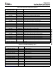
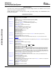
Table 7-100. PCI Hook Configuration Registers
DSP ACCESS
ACRONYM DSP ACCESS REGISTER NAME
HEX ADDRESS RANGE
02C0 0394 PCIVENDEVPRG PCI Vendor ID and Device ID Program Register
02C0 0398 PCICMDSTATPRG PCI Command and Status Program Register
02C0 039C PCICLREVPRG PCI Class Code and Revision ID Program Register
02C0 03A0 PCISUBIDPRG PCI Subsystem Vendor ID and Subsystem ID Program Register
02C0 03A4 PCIMAXLGPRG PCI Max Latency and Min Grant Program Register
02C0 03A8 PCILRSTREG PCI LRESET Register
02C0 03AC PCICFGDONE PCI Configuration Done Register
02C0 03B0 PCIBAR0MPRG PCI Base Address Mask Register 0 Program Register
02C0 03B4 PCIBAR1MPRG PCI Base Address Mask Register 1 Program Register
02C0 03B8 PCIBAR2MPRG PCI Base Address Mask Register 2 Program Register
02C0 03BC PCIBAR3MPRG PCI Base Address Mask Register 3 Program Register
02C0 03C0 PCIBAR4MPRG PCI Base Address Mask Register 4 Program Register
02C0 03C4 PCIBAR5MPRG PCI Base Address Mask Register 5 Program Register
02C0 03C8 PCIBAR0PRG PCI Base Address Register 0 Program Register
02C0 03CC PCIBAR1PRG PCI Base Address Register 1 Program Register
02C0 03D0 PCIBAR2PRG PCI Base Address Register 2 Program Register
02C0 03D4 PCIBAR3PRG PCI Base Address Register 3 Program Register
02C0 03D8 PCIBAR4PRG PCI Base Address Register 4 Program Register
02C0 03DC PCIBAR5PRG PCI Base Address Register 5 Program Register
02C0 03E0 PCIBAR0TRLPRG PCI Base Address Translation Register 0 Program Register
02C0 03E4 PCIBAR1TRLPRG PCI Base Address Translation Register 1 Program Register
02C0 03E8 PCIBAR2TRLPRG PCI Base Address Translation Register 2 Program Register
02C0 03EC PCIBAR3TRLPRG PCI Base Address Translation Register 3 Program Register
02C0 03F0 PCIBAR4TRLPRG PCI Base Address Translation Register 4 Program Register
02C0 03F4 PCIBAR5TRLPRG PCI Base Address Translation Register 5 Program Register
02C0 03F8 PCIBASENPRG PCI Base En Prog Register
02C0 03FC - 02C0 03FF - Reserved
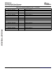
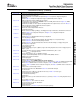
Table 7-101. PCI External Memory Space
HEX ADDRESS OFFSET ACRONYM REGISTER NAME
4000 0000 - 407F FFFF - PCI Master Window 0
4080 0000 - 40FF FFFF - PCI Master Window 1
4100 0000 - 417F FFFF - PCI Master Window 2
4180 0000 - 41FF FFFF - PCI Master Window 3
4200 0000 - 427F FFFF - PCI Master Window 4
4280 0000 - 42FF FFFF - PCI Master Window 5
4300 0000 - 437F FFFF - PCI Master Window 6
4380 0000 - 43FF FFFF - PCI Master Window 7
4400 0000 - 447F FFFF - PCI Master Window 8
4480 0000 - 44FF FFFF - PCI Master Window 9
4500 0000 - 457F FFFF - PCI Master Window 10
4580 0000 - 45FF FFFF - PCI Master Window 11
4600 0000 - 467F FFFF - PCI Master Window 12
4680 0000 - 46FF FFFF - PCI Master Window 13
4700 0000 - 477F FFFF - PCI Master Window 14
Submit Documentation Feedback C64x+ Peripheral Information and Electrical Specifications 211