
User's Manual


www.ti.com
PRODUCT PREVIEW
Revision History
TMS320C6454
Fixed-Point Digital Signal Processor
SPRS311A – APRIL 2006 – REVISED DECEMBER 2006
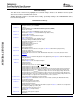
This data sheet revision history highlights the technical changes made to the SPRS311 device-specific
data sheet to make it an SPRS311A revision.
Scope: Applicable updates to the C64x device family, specifically relating to the TMS320C6454 device,
have been incorporated.
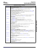
C6454 Revision History
SEE ADDITIONS/MODIFICATIONS/DELETIONS
Global Changed DDR2 Memory Controller speed to 533 MHz
Changed L2 Memory size to 1048KB
Section 1.1 Features:
Changed EMIFA bullet to 64-Bit External Memory Interface (EMIFA)
Added 1.25-V Internal
Section 1.1.1 Change section title to ZTZ /GTZ BGA Package (Bottom View):
Added GTZ to Section 1.1.1 , ZTZ/GTZ BGA Package (Bottom View)
Section 1.3 Functional Block Diagram:
Updated Figure 1-2 , Functional Block Diagram
Section 2.1 Device Characteristics:
Table 2-1 , Characteristics of the C6454 Processor:
Deleted [133 MHz] from EMIFA (64-bit bus width)
Changed On-Chip Memory Size to 1144K
Updated Core Voltages
Updated Megamodule Revision ID
Updated JTAG BSDL_ID
Added GTZ Package
Section 2.3 Memory Map Summary:
Added EDMA Transfer Controller 0-3 Registers to Table 2-2 , C6454 Memory Map Summary
Section 2.4.1 Boot Modes Supported:
Updated paragraphs under Host boot bullet
Replaced TBD document reference with TMS320C645x Bootloader User's Guide (literature number
SPRUEC6 )
Section 2.5.1 Pin Map:
Updated Figure 2-4 , C6454 Pin Map (Bottom View) [Quadrant C] and Figure 2-5 , C6454 Pin Map (Bottom
View) [Quadrant D]
Section 2.6 Signal Groups Description:
Updated Figure 2-6 , CPU and Peripheral Signals
Table 2-3 Terminal Functions:
Updated Footnote (2)
Added footnote (5) reference to Signals PSERR and PINTA
Updated Signal Description for AR/ W
Updated Signal Description for DEODT1 and DEODT2
Updated Signal Descriptions for RSV07, RSV09, RSV15, RSV16, RSV32, RSV33, RSV34, and RSV35
Changed Signal N1 to CV
DDMON
, updated Description, and moved under Supply Voltage Monitor Pins
Changed Signal L6 to DV
DD33MON
, updated Description, and moved under Supply Voltage Monitor Pins
Changed Signal F3 to DV
DD15MON
, updated Description, and moved under Supply Voltage Monitor Pins
Changed Signal A26 to DV
DD18MON
, updated Description, and moved under Supply Voltage Monitor Pins
Updated Descriptions for Signals AV
DDA
, DV
DDRM
, DV
DD12
, AV
DDT
, and CV
DD
Section 2.8.2.1 Device and Development-Support Tool Nomenclature:
Updated Figure 2-12 , TMS320C64x+ DSP Device Nomenclature (including the TMS320C6454 DSP)
Section 2.8.2.2 Documentation Support:
Updated list of related documentation
Section 3.1 Device Configuration at Device Reset:
Updated paragraph and Note
Updated Footnote (1) and Configuration Pin AEA3 Description in Table 3-1 , C6454 Device Configuration
Pins (AEA[19:0], ABA[1:0], and PCI_EN)
Section 3.3 Peripheral Selection After Device Reset:
Updated Table 3-4 , Peripheral States
Added Note
Section 3.4.1 Peripheral Lock Register Description:
Added Note
Revision History218 Submit Documentation Feedback