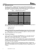
TVP5160EVM User’s Guide SLEU063 – March 2005 TVP5160EVM User’s Guide Digital Video Department 1 2 3 4 5 6 7 8 9 10 Contents Functional Description......................................................................................................................3 1.1 Description Overview ...................................................................................................................3 Board Level Description ..........................................................................
SLEU063 Figure 1. Figure 2. Figure 3. Figure 4. Figure 5. Figure 6. Figure 7. Figure 8. Figure 9. Figure 10. Figure 11. Figure 12. Figure 13. Figure 14. Figure 15. Figure 16. Figure 17. Figure 18. Figure 19. Figure 20. Figure 21. Figure 22. Figures TVP5160EVM Block Diagram.............................................................................................. 4 TVP5160EVM System Level Block Diagram .....................................................................
SLEU063 1 Functional Description The TVP5160EVM refers to both the TVP5160 board and the ADV7311 board when they are connected together. Both boards share a common interface via a 120-pin connector. This interface provides all data, clocks, I2C communication, and 5-V power to each board. The ADV7311 is a professional grade, 12-bit, 216-MHz, video encoder. This device minimizes potential artifacts caused by the re-encode process.
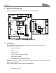
SLEU063 2 Board Level Description Figure 1 illustrates the various features available on the TVP5160EVM. DB25 (I2C) 5V Power Analog Output Power Good LED Tuner Interface VBI Decoder Interface TVP5160 YPbPr (SD/ED) Power Down Testpoints S-Video 120-pin Header Connector Composite 120-pin Header Connector Composite Power Good LED Reset YPbPr (SD/ED) Testpoints Reset FSS I2C Select Address Select Figure 1. 2.
SLEU063 Table 1. Analog Inputs and Pin Terminals Input Type 2.2 TVP5160 Pin(s) CVBS VI_1 S-Video VI_3(Y), VI_9(C) YPbPr VI_5(Y), VI_11(Pb), VI_8(Pr) SCART VI_3(CVBS), VI_9(R), VI_6(G), VI_12(B) Tuner interface (CVBS) VI_2 VBI decoder interface (analog RGB) VI_7(R), VI_4(G), VI_10(B) Anti-Aliasing Filters Each analog input has an anti-alias filter installed by default to ensure the input to the TVP5160 decoder is of the best quality and does not alias.
SLEU063 2.5 VBI Decoder Interface This interface provides a method of connecting an external VBI decoder module to the TVP5160EVM via the H3 and H4 headers. The VBI decoder may be a closed-caption decoder, teletext decoder, or any other VBI decoder currently available on the market that provides the same signals. The pinout of the VBI decoder interface is provided below. Table 3.
SLEU063 2.7 SDRAM On the TVP5160EVM, there are three SDRAM footprints: 50-pin, 54-pin, and 86-pin. These are provided to accommodate the user’s choice of SDRAM that will be used in their final product. By default, the TVP5160EVM is provided with 64-Mbit SDRAM (54TSOPII). If the SDRAM is changed, then the SDRAM configuration register (0x59) will also need to be updated with the correct memory size. This must be programmed before 3DYC or 3DNR is enabled. 2.
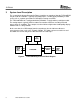
SLEU063 3 System Level Description The system block diagram illustrated in Figure 2 provides an example of how the TVP5160EVM may be used for evaluation. Typically, the analog input is a CVBS signal provided by a video source such as a pattern generator or a DVD player running a test DVD. The TVP5160EVM itself is configured with the provided 5-V supply and the parallel port cable. The analog output is typically YPbPr to reduce the number of artifacts caused by backend processing or re-encoding.
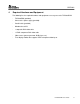
SLEU063 4 Required Hardware and Equipment The following lists the required hardware and equipment necessary to use the TVP5160EVM: - TVP5160EVM (provided) - Universal 5-V power supply (provided) - Parallel cable (provided) - Windows-based PC - 1 composite RCA video cable - 1 YPbPr component RCA video cable - Video source (pattern generator, DVD player, etc) - TV or display monitor that supports YPbPr component video inputs TVP5160EVM User’s Guide 9
SLEU063 5 Hardware Setup The following describes how to set up the hardware for the TVP5160EVM. 1. Connect the TVP5160EVM boards together using the 120-pin board connector on each board. 2. Connect a CVBS input to the TVP5160 board and a component cable to the YPbPr outputs of the ADV7311 board. NOTE: For evaluation it is recommended that the YPbPr component video outputs be used in order to bypass the internal video decoder of the TV or video display. 3.
SLEU063 6 Software Installation WinVCC4 is a Windows application that uses the PC parallel port to emulate I2C, providing access to each device on the I2C bus. WinVCC4 makes use of CMD files, a text editable file that allows preset video setups to be programmed easily. This feature allows the user to easily set multiple I2C registers with the press of a button. WinVCC4 also has “Property Sheets” for the TVP5160 which allows the user to control the I2C registers with a GUI.
SLEU063 7 WinVCC4 Quick Start The following describes the steps to take within WinVCC4 in order to get video out of the TVP5160EVM. 1. Once WinVCC4 is executed, the WinVCC4 Configuration screen appears. This dialog box is used to configure the I2C bus. Next to VID_DEC, select the TVP5160 and ensure the I2C address is set to 0xB8. This should match the I2C ADDR jumper on the TVP5160 board. NOTE: If WinVCC4 is running and the TVP5160 board I2C address is changed, power must be cycled on the EVM. Figure 3.
SLEU063 5. At the Real-Time Polling window, ensure that VIDEO-STANDARD AUTO_SWITCH POLLING is enabled and click OK. Figure 4. WinVCC4 – Real Time Polling Screen 6. Load the provided TVP5160EVM.CMD file into WinVCC4 by clicking on Tools -> System Initialization -> Browse. The CMD should be available by default as seen below. Figure 5. WinVCC4 – Main Screen 7. Click the “TVP5160 (SD) + ADV7311” dataset in the window and then click the Program Dataset button to initialize the TVP5160EVM. Figure 6.
SLEU063 8. With a video source provided at the composite video input, video should be viewable on the TV/display monitor. All ADV7311 outputs are enabled simultaneously. NOTE: To ensure the TVP5160 is working properly, go to Video Status by clicking on Edit -> Property Sheets -> TVP5160PNP -> Video Decoder Status and check the H/V/C lock status and the video standard. This is only a check on the TVP5160 board and not the ADV7311 board or the TV/display monitor.
SLEU063 8 WinVCC4 in Depth The following describes how to use WinVCC4 in depth. It discusses various features and screens which the user m ay encounter while evaluating the TVP5160EVM. 8.1 Starting WinVCC4 The Port95NT parallel port driver must be installed before using WinVCC4. WinVCC4 may be started by clicking on Start->All Programs->TVP5160EVM Software->WinVCC4. If the dialog shown in the figure below is displayed, it means one of two things: 1.
SLEU063 8.2 WinVCC4 Configuration Dialog Box The WinVCC4 Configuration dialog box, as seen in Figure 8, should now be visible. This dialog configures the I2C bus on the TVP5160EVM. All settings from this dialog box are stored in the Windows registry and are restored the next time the program is started. After initial installation, VID_DECTM will be set to TVP5160 and VID_ENC will be set to ADV7311. The I2C slave address for each device must match the I2C slave address selected by jumpers on the TVP5160EVM.
SLEU063 8.3 I2C System Test The I2C system test of selected registers runs immediately after closing the WinVCC4 Configuration dialog box with OK (unless the I2C system test program options button was disabled). If the I2C system test passes, then only a PASS message will appear. If the test failed, then a dialog box like Figure 9 will appear. See Section 9, Troubleshooting, for details on how to resolve this issue.
SLEU063 If the WinVCC4 autoswitch polling function is enabled, then the detected video standard status from the TVP5160 decoder is polled until a change in the input video standard (or in the TVP5160 sampling mode) is detected. When a change is detected, the video encoder is reprogrammed as needed for the detected standard. Using this feature, the video source can change its video standard and the system will display using the new standard without user intervention.
SLEU063 8.5 Main Menu After closing the Real–Time Polling dialog, the main menu is displayed as shown in Figure 11. The menus, which are used to operate WinVCC4, are File, Edit, Tools, Window, and Help. The File menu’s only function is Exit, which terminates the program. The following table summarizes the main menu contents. Figure 11. WinVCC4 – Main Screen Table 4.
SLEU063 8.5.1 System Initialization Clicking System Initialization in the Tools menu displays the dialog shown below. This provides the means for initializing the video decoder and/or video encoder for a particular video mode. The details of the initialization are contained in the command file (with a CMD file extension). The command file is loaded using the Browse… button. Once the command file is opened, a text list displays descriptions of the individual data sets contained within the command file.
SLEU063 8.5.1.1 Adding a Custom Data Set After you program the EVM via the System Initialization tool using the factory-supplied command file, and by using the Property Sheets tool, you can customize the device register settings to suit your needs. To save your custom settings: 1. Reopen the System Initialization dialog via the Tools menu. 2. Click the Append Current Device Settings to Command File button. A dialog requesting a description of the new data set appears. 3.
SLEU063 8.5.1.3 Example Command File An example of one data set within a command file is shown below. Each command file may contain individual write to register (WR_REG) commands.
SLEU063 7.
SLEU063 8.5.2 Register Editing The next section describes the four available modes of register editing: Register Map Editor, Encoder Module Editor, Generic I2C Register Editor, and Property Sheets. Each of these functions can be selected from the Edit menu. 8.5.2.1 Register Map Editor The register map editor, as shown in Figure 13, allows the display and editing of the entire used register space of the device within a simple scrolling text box.
SLEU063 Table 5. Control Register Map Editor Controls Definition Register Window Scrolling text box that displays the address and data for the I2C registers that are defined for the device. Address Edit Box This contains the I2C subaddress that will be accessed using the Write and Read buttons. Clicking on a row selects an address, which then appears in the address edit box. NOTE: After clicking on a row, the Data Edit box contains the data that was in the register window.
SLEU063 8.5.2.2 Encoder Module Editor The encoder module editor, as shown in Figure 14, allows the display and editing of the video encoder registers. This editor works like the Register Map Editor. To open this, click on Edit Register Map in the Edit menu and click on Encoder Module. Figure 14.
SLEU063 8.5.2.3 Generic I2C Register Editor The Generic I2C Editor, as shown in Figure 15, allows the display and editing of any device on the I2C bus. This editor works like the Register Map Editor, except that the I2C slave address must be entered and the Read All button is disabled. To open this, click on Edit Register Map in the Edit menu and then click on Generic I2C.
SLEU063 8.5.2.4 Indirect Register Editor The indirect register editor, as shown in Figure 16, allows the display and editing of the indirect registers (or hardware registers) of the device. To open this, first open the register map editor in the Edit menu for the TVP5160. Then, click the Edit Indirect Registers button. The operation of the controls of the indirect register editor is explained in Table 6. Figure 16. Indirect Register Editor Table 6.
SLEU063 8.5.3 Property Sheets The Property Sheets represent the register data in a user-friendly format. The data is organized by function, with each function having its own page and being selectable via tabs at the top. To open this, click on Edit Property Sheets in the Edit menu and select the device type to edit. When the property sheet function is started or whenever you tab to a different page, all readable registers in the device are read from hardware to initialize the dialog pages.
SLEU063 8.5.3.2 Auto–Update from Device Items 4 and 5 above are referred to as the Auto–Update feature. Auto–Update can be disabled by setting its program option button to DISABLED. This button is located on the initial dialog box (WinVCC4 Configuration). With Auto–Update enabled (default), the user can open both the Property Sheets and the Register Map Editor at the same time.
SLEU063 Table 7.
SLEU063 9 Troubleshooting This chapter discusses ways to troubleshoot the TVP5160EVM. 9.1 Troubleshooting Guide If you are experiencing problems with the TVP5160EVM hardware or the WinVCC4 software, see Table 9 for available solutions. Table 9. Symptom TVP5160EVM Troubleshooting Cause Solution At startup, the error message Cannot find DLL file DLPORTIO.DLL appears. The parallel port driver supplied with the EVM has not been installed. Run Port95NT.EXE on the CD to install the driver.
SLEU063 Table 10. Symptom 2 No I C communication I2C Troubleshooting Cause 2 Solution I C slave address is wrong. Close and restart WinVCC4. Choose the alternate slave address in the WinVCC4 Configuration dialog. Parallel cable is not connected from PC parallel port to the EVM DB25 connector. Connect cable. EVM is not powered on. The power supply must be plugged into a 100-V to 240-V/ 47-Hz to 63-Hz power source and the cord must be plugged into the power connector on the EVM.
SLEU063 Figure 18. I2C System Failure Dialog Box 9.2 Corrective Action Dialogs After closing the I2C system test report dialog box, the dialog in Figure 19 appears. Figure 19. Corrective Action Dialog Box 1. If the cable is NOT connected from the PC parallel port to the TVP5160EVM or if the EVM power is not on: a. Click NO. b. The dialog shown in Figure 20 appears instructing you to correct the problem.
SLEU063 c. Correct the problem. d. Click OK to continue. The real-time polling dialog should appear. See Section 3.2.3. Figure 20. Corrective Action Required 2. If the cable is connected from the PC parallel port to the TVP5160EVM AND the EVM power is on: a. Click Yes. b. The dialog shown in Figure 21 appears. This dialog appears if the PC parallel port mode setting may need to be changed. NOTE: Only run the PC BIOS setup program if the I2C communication problem cannot be resolved in another way.
SLEU063 1. Restart the PC. 2. During the boot process, enter the BIOS setup program by pressing the required key (usually the initial text screen tells you which key to press). 3. Find the place where the parallel port settings are made. 4. Set the parallel port LPT1 at address 378h to ECP mode or bidirectional mode (sometimes called PS/2 mode or byte mode). If one of these two modes is already selected, change to the opposite mode. 5. Exit and save changes. 9.2.
SLEU063 10 TVP5160EVM Schematics This chapter contains the TVP5160EVM schematics.
1 2 3 4 5 6 ADV7311 Board Revision 1.0 D D Feb 2005 Connector Connector C SCL SDA CONN_RESET RESET ADV7311 MODULE REV 1.0 Power Power I2C I2C C ADV7311 ADV7311 CONN_RESET G/Y /RESET SCL SDA SCL SDA Y[9..0] CLKIN /HSYNC /VSYNC /BLANK Y[9..0] CLKIN /HSYNC /VSYNC /BLANK UV[9..0] C[9..0] B/Pb R/Pr RTC RTC SV DVI Tx DVI Tx B CVBS RTC SCL SDA Y[9..0] UV[9..
1 2 3 4 5 6 D D D3_3V C1 0.1uF R2 2.2k 2.2k R1 R3 2.2k C 27 C P3 U2C 1 14 2 15 3 16 4 17 5 18 6 19 7 20 8 21 9 22 10 23 11 24 12 25 13 U2D 6 5 9 R6 SCL SCL 0 74AHC05 DB15 74AHC05 U2F DB17 13 12 D3_3V 74AHC05 U2A 1 2 74AHC05 7 DB9 R8 2.2k 14 R7 2.2k DB11 U2B 4 26 8 DB25F R4 2.2k 3 0 SDA SDA R9 R5 2.2k 74AHC05 B B U2E 11 10 74AHC05 A A Title ENCODER EVM - I2C Size Number Revision C Date: File: 1 2 3 4 5 REV 1.
1 2 3 4 5 6 D D OPTIONAL 5V, 3.0A DC INPUT MAIN SUPPLY FROM CONNECTOR D5V F1 P1 PJ-002BH FUSE L1 H1 1 3 2 C 3 2 1 D1 ZENER A5V C2 47uF L2 C3 22uF A3_3V C6 22uF C7 0.1uF C SS26 HEADER 3 D5V U1 1 2 3 C4 1uF POWER ON LED (+5V) D3_3V IN OUT GND BYPASS 5 4 EN TPS76233 C5 0.
1 2 3 4 5 6 D D Y[9..0] Y[9..0] H2 Y0 Y1 Y2 Y3 Y4 Y5 Y6 Y7 Y8 Y9 C 1 3 5 7 9 11 13 15 17 19 2 4 6 8 10 12 14 16 18 20 C HEADER 10X2 UV[9..0] UV[9..
1 2 3 4 5 6 D D D5V D5V D5V D5V P2 SCL SDA C SCL SDA 30 29 28 27 26 25 24 23 22 21 20 19 18 17 16 15 14 13 12 11 10 9 8 7 6 5 4 3 2 1 60 59 58 57 56 55 54 53 52 51 50 49 48 47 46 45 44 43 42 41 40 39 38 37 36 35 34 33 32 31 5V 5V GND GND GND SCL/PHI_ACK SDA/PHI_RWW PHI_DS/RD PHI_CS PHI_A1 PHI_A0 PHI_D7 PHI_D6 PHI_D5 PHI_D4 PHI_D3 PHI_D2 PHI_D1 PHI_D0 GND CLK5/M1 FPDAT/VSYA/M2 FFRSTW/CBFLAG FSY/HC/HSYA/~BLNK VGAV/SYNC_T FFIE/CCVALID FFWE/DVALID FFRSTWIN/~SCLK FFRE/DIG_H FFOE/DIG_V 5V 5V GN
1 2 D3_3V 3 4 5 A3_3V 6 C17 C14 0.1uF U4A AD8062 L3 I2C ADDRESS SELECTION CVBS 3 10uH R15 604 1-2 Base Addr 0x56 1 C15 NO POP C19 R17 604 2 CVBS RCA R21 2 75 22pF 2-3 Base Addr 0x54 - Default C21 R23 D C23 1uF NO POP A5V 1 C13 0.1uF 8 C12 0.1uF 4 NO POP C11 0.1uF 0 C24 0.
2 3 TVP5160EVM Rev 2.0 AOUT Revision 2.0 6 Power Power I2C I2C Feb 2005 D Tuner Interface Tuner Interface VBI Decoder Interface VBI Decoder Interface DG DB DR FSO CVBS VSYNC HSYNC DG DB DR FSO SCL SDA T_CVBS CVBS_IN SCL SDA TUNER_CVBS GREEN BLUE RED FSS_RGB Tuner SCL SDA Connector Connector TUNER_CVBS C Anti-Aliasing Filters Anti-Aliasing Filters CVBS_IN CVBS_OUT Y_IN C_IN Y_OUT C_OUT Y/G_IN Pb/B_IN Pr/R_IN Y/G_IN Pb/B_IN Pr/R_IN Y/G_OUT Pb/B_OUT Pr/R_OUT C[9..0] Y[9..
1 2 3 4 5 6 D D D3_3V C1 T2 TP POUT TP T1 TP NACK TP TP T0 0.1uF C 1 1 1 1 R52 2.2k 27 1 R24 2.2k 2.2k R8 C P3 U2C U2D 6 5 26 9 R6 SCL 0 DB15 74AHC05 U2F 13 DB17 12 D3_3V 74AHC05 U2A 1 DB9 R9 2.2k 14 R7 2.2k 2 74AHC05 DB11 U2B 4 DB25 8 74AHC05 7 1 14 2 15 3 16 4 17 5 18 6 19 7 20 8 21 9 22 10 23 11 24 12 25 13 R53 2.2k 0 3 SDA SDA R5 R54 2.
1 2 3 4 5 6 D D D5V H2 C TUNER_CVBS 2 4 6 8 10 12 14 16 18 20 22 24 26 28 30 32 34 36 38 40 1 3 5 7 9 11 13 15 17 19 21 23 25 27 29 31 33 35 37 39 C SDA SCL SAMTEC SSW-120-02-G-D B B A A Title TVP5146EVM - TV TUNER INTERFACE Size Number Revision REV 2.0 C Date: File: 1 2 3 4 5 16-Feb-2005 Sheet of C:\Userdata\EVM Design Files\MODULARIZED_EVMS\TVP5160EVM\TVP5160EVM_MODULE_REV2.0\TVP5160EVM_MODULE_REV Drawn By: 2.0.
1 2 3 4 6 5 D D D5V C R60 0 T_CVBS CVBS_IN BLUE GREEN RED H3 1 3 5 7 9 11 C H4 2 4 6 8 10 12 HSYNC VSYNC FSS_RGB SAMTEC SSW-106-02-G-D DR DG DB 1 3 5 7 9 11 2 4 6 8 10 12 SDA SCL FSO SAMTEC SSW-106-02-G-D B B A A Title TVP5160EVM - VBI DECODER INTERFACE Size B Date: File: 1 2 3 4 5 Number Revision REV 2.0 16-Feb-2005 Sheet of C:\Userdata\EVM Design Files\MODULARIZED_EVMS\TVP5160EVM\TVP5160EVM_MODULE_REV2.
1 2 3 4 6 5 D D COMPONENT - YPbPr Y/G_IN Y/G_IN C3 5.6pF L1 1.8uH Y/G_OUT C7 220pF C Pr/R_IN Pr/R_IN C6 8.2pF L2 2.2uH CVBS & S-VIDEO Y/G_OUT CVBS_IN CVBS_IN C9 220pF L7 Pr/R_OUT Pr/R_OUT Y_IN Y_IN C10 330pF 1.8uH C16 8.2pF CVBS_OUT CVBS_OUT SCRT_GRN_IN SCRT_GRN_IN C14 220pF L4 2.2uH C13 330pF L6 2.2uH SCRT_GRN_OUT C18 330pF SCRT_GRN_OUT C20 330pF C C27 8.2pF Y_OUT Y_OUT SCRT_BLUE_IN C15 330pF SCRT_BLUE_IN L9 2.
1 2 3 4 5 6 D D 5V, 3.0A DC INPUT D5V FUSE L11 A5V 2 F1 P1 PJ-002BH C33 47uF H1 D1 ZENER 3 2 1 HEADER 3 C34 22uF SS26 1 1 3 2 TVP5160 POWER SUPPLY VOUT1 IS 3.3V 1A VOUT2 IS 1.8V 2A L12 A3_3V C39 47uF R20 249k C C35 22uF D5V C37 0.1uF R19 330 C36 22uF 0 C38 0.
1 2 3 4 6 5 D3_3V C51 0.1uF C52 0.1uF C53 0.1uF C54 0.1uF C55 0.1uF C56 0.1uF D D DQ[15..0] DQ[15..
1 2 3 4 6 5 D3_3V C57 0.1uF C58 0.1uF C59 0.1uF C60 0.1uF C61 0.1uF C62 0.1uF C63 0.1uF C64 0.1uF C65 0.1uF C66 0.1uF C67 0.1uF C68 0.1uF D D DQ[15..0] DQ[15..
1 2 3 4 6 5 D3_3V C69 0.1uF C70 0.1uF C71 0.1uF C72 0.1uF C73 0.1uF C74 0.1uF C75 0.1uF D D DQ[15..0] DQ[15..
1 2 3 4 5 6 D D D5V D5V D5V D5V P2 C SCL SDA 30 29 28 27 26 25 24 23 22 21 20 19 18 17 16 15 14 13 12 11 10 9 8 7 6 5 4 3 2 1 5V 5V GND GND GND SCL/PHI_ACK SDA/PHI_RWW PHI_DS/RD PHI_CS PHI_A1 PHI_A0 PHI_D7 PHI_D6 PHI_D5 PHI_D4 PHI_D3 PHI_D2 PHI_D1 PHI_D0 GND INTREQU CLK5/M1 FPDAT/VSYA/M2 FFRSTW/CBFLAG FSY/HC/HSYA/~BLNK VGAV/SYNC_T FFIE/CCVALID FFWE/DVALID FFRSTWIN/~SCLK FFRE/DIG_H FFOE/DIG_V INTREQU 60 59 58 57 56 55 54 53 52 51 50 49 48 47 46 45 44 43 42 41 40 39 38 37 36 35 34 33 32 31
1 2 3 4 5 6 D D D5V H6 C SCL SDA Y[9..0] GND2 GND Y9 Y8 Y7 Y6 Y5 Y4 Y3 Y2 Y1 Y0 C[9..0] C9 C8 C7 C6 C5 C4 C3 C2 C1 C0 2 4 6 8 10 12 14 16 18 20 22 24 26 28 30 32 34 36 38 40 VS_VBLNK HSYNC FID AVID DATACLK GLCO INTREQ_TP C C[9..0] VSYNC HSYNC FID AVID DATACLK GLCO INTREQ_TP TP D1.8V 1_8V A1_8V A1.8V 1_8V D1_8V S_CVBS_OUT TP A3.3V 3_3V 1 D3.3V 3_3V TP A3_3V 1 1 D3_3V TP TP A5V A5V 1 A5V Y[9..
1 2 A1_8V 3 4 5 6 A3_3V A5V C78 0.1uF C80 0.1uF C82 0.1uF C86 0.1uF C88 0.1uF C90 0.1uF R27 22 R29 12k Q1 ANALOG RCA C81 0.1uF C83 0.1uF C84 0.1uF C85 0.1uF C87 0.1uF C89 0.1uF C91 0.1uF C92 0.1uF C93 0.1uF 2 ANALOG_OUT R30 22k 75 D 22uF 2N2222 AOUT R26 1 R28 1k A1_8V CVBS RCA A3_3V 1 2 JP1 2 128 127 126 125 124 123 122 121 120 119 118 117 116 115 114 113 112 111 110 109 108 107 106 105 104 103 102 101 100 99 98 97 0.1uF C97 0.1uF C98 0.1uF Y/G C99 0.
IMPORTANT NOTICE Texas Instruments Incorporated and its subsidiaries (TI) reserve the right to make corrections, modifications, enhancements, improvements, and other changes to its products and services at any time and to discontinue any product or service without notice. Customers should obtain the latest relevant information before placing orders and should verify that such information is current and complete.