
User's Manual


Functional Description
59
SLES140A—March 2007 TVP5147M1PFP
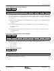
2.11.59 Analog Output Control 1 Register
Subaddress 7Fh
Default 00h
7 6 5 4 3 2 1 0
Reserved AGC enable Input select Analog Output enable
AGC enable:
0 = Enabled (default)
1 = Disabled, manual gain mode (see Section 2.12.10)
Input select:
00 = Input selected by TVP5147M1 decoder, (see Section 2.11.1) (default)
01 = Input selected manually (see Section 2.12.10)
Analog output enable:
0 = VI_1_A is input (default).
1 = VI_1_A is analog video output.
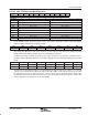
2.11.60 Chip ID MSB Register
Subaddress 80h
Read only
7 6 5 4 3 2 1 0
Chip ID MSB [7:0]
Chip ID MSB [7:0]: This register identifies the MSB of the device ID. Value = 51h
2.11.61 Chip ID LSB Register
Subaddress 81h
Read only
7 6 5 4 3 2 1 0
Chip ID LSB [7:0]
Chip ID LSB [7:0]: This register identifies the LSB of the device ID. Value = 47h
2.11.62 CPLL Speed Control Register
Subaddress 83h
Default 09h
7 6 5 4 3 2 1 0
Reserved Speed [3:0]
Speed [3:0]: Color PLL speed control
1001 = Faster (default)
1010 =
1011 = Slower
Other = Reserved