
User Manual

Theia lens motor controller instructions
Theia Technologies® motor control
v.180628
The I2C signals have 4.7 kOhm pull-up resistors on board. Speeds up to 400 kBaud are supported. ESD protection is
provided to these signals by Littelfuse®** SP724AHTG clamping diode arrays. Please see its datasheet for details.
Similar boards with I2C voltage level translation to 1.8V or 3.3V are available.
*/ Molex is a trademark of Molex LLC, USA
**/ Littelfuse is a trademark of Littelfuse Inc., USA
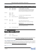
3.3. UART (J2)
J2 is a Molex®* 53047-0610 or compatible connector. The fitting cable connector might be the Molex®*
51021-0600 or compatible.
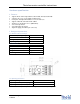
J2 has a total of 6 circuits (pins) of which the UART interface uses two for its signals. To function the board would
additionally need a ground reference (GND) and a 5V power supply. Both are available on J2 as well.
1 – UART TxD
2 – UART RxD
5 – Power GND
6 – Power +5 V
The UART signals run at (5V CMOS) TTL levels at 19200 Baud and are 8N1 encoded. Please ask if you need that to be
changed to something else. Similar boards with RS232 signal levels are available.
ESD protection is provided to these signals by Littelfuse®** SP724AHTG clamping diode arrays. Please see its
datasheet for details.
*/ Molex is a trademark of Molex LLC, USA
**/ Littelfuse is a trademark of Littelfuse Inc., USA
3.4. SPI (JP1)
JP1 is 3x2 pin header with 2.54 mm (0.1”) spacing. This header is normally used for the initial firmware upload to the
controller, but this happens through an SPI bus which could be made available to clients as a means to communicate
with the board. At the moment that support is not yet implemented. Please ask if it is needed.
JP1 has a total of 6 circuits (pins) of which the SPI interface uses three for its signals. To function the board would
additionally need a ground reference (GND) and a 5V power supply. Both are available on JP1 as well.
1 – SPI MISO
2 – Power +5 V
3 – SPI SCK
4 – SPI MOSI
5 – Reset
6 – Power GND
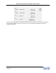
6
5
4
3
2
1
J 2
6
5
4
3
2
1
JP 1