
Secure Digital Card Datasheet

S
S
S
D
D
D
H
H
H
C
C
C
C
C
C
a
a
a
r
r
r
d
d
d
s
s
s
e
e
e
r
r
r
i
i
i
e
e
e
s
s
s
4~32GB High Capacity Secure Digital Card
Transcend Information Inc.
5
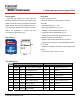
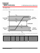
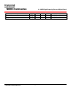
• Bus Signal Levels
As the bus can be supplied with a variable supply voltage, all signal levels are related to the supply voltage.
To meet the requirements of the JEDEC specification JESD8-1A and JESD8-7, the card input and output voltages shall be
within the following specified ranges for any V
DD
of the allowed voltage range:
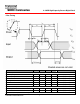
Parameter Symbol Min. Max. Unit Remark
Output HIGH voltage V
OH
0.75* V
DD
V I
OH
= -100 μA @V
DD
min
Output LOW voltage V
OL
0.125* V
DD
V I
OL
= -100 μA @V
DD
min
Input HIGH voltage V
IH
0.625* V
DD
V
DD
+ 0.3 V
Input LOW voltage V
IL
V
SS
– 0.3 0.25* V
DD
V