T Trraan nsscceen nd d IIn nd du ussttrriiaall C CF FC Caarrd d ((T TS S112288M M ~~ 1166G GC CF F110000II)) Description Features The Transcend CF100I is a High Speed industrial • CompactFlash Specification Version 4.1 Complaint Compact Flash Card with high quality Flash Memory • RoHS compliant products assembled on a printed circuit board. • Single Power Supply: 3.
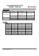
T Trraan nsscceen nd d IIn nd du ussttrriiaall C CF FC Caarrd d ((T TS S112288M M ~~ 1166G GC CF F110000II)) Order information Part Number Interface Transfer Mode Ultra DMA mode 0~4 True IDE mode TS128M~16GCF100I TS128M~16GCF100I-P Multi-Word DMA Mode 0~4 Fixed Disk (Standard) PIO Mode 0 ~ 6 PC Card mode (PCMCIA) 80ns, 100ns, 120ns, 250ns Fixed Disk (Standard) True IDE mode Fixed Disk (Standard) PIO Mode 0 ~ 4 PC Card mode (PCMCIA) 250ns Fixed Disk (Standard) C.H.S.
T Trraan nsscceen nd d IIn nd du ussttrriiaall C CF FC Caarrd d ((T TS S112288M M ~~ 1166G GC CF F110000II)) Transcend Transcend Information Inc. 3 V1.
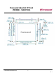
T Trraan nsscceen nd d IIn nd du ussttrriiaall C CF FC Caarrd d ((T TS S112288M M ~~ 1166G GC CF F110000II)) Block Diagram Transcend Information Inc. 4 V1.
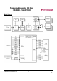
T Trraan nsscceen nd d IIn nd du ussttrriiaall C CF FC Caarrd d ((T TS S112288M M ~~ 1166G GC CF F110000II)) Pin Assignments and Pin Type Transcend Information Inc. 5 V1.
T Trraan nsscceen nd d IIn nd du ussttrriiaall C CF FC Caarrd d ((T TS S112288M M ~~ 1166G GC CF F110000II)) Note: 1) These signals are required only for 16 bit accesses and not required when installed in 8 bit systems. Devices should allow for 3-state signals not to consume current. 2) The signal should be grounded by the host. 3) The signal should be tied to VCC by the host. 4) The mode is required for CompactFlash Storage Cards. 5) The -CSEL signal is ignored by the card in PC Card modes.
T Trraan nsscceen nd d IIn nd du ussttrriiaall C CF FC Caarrd d ((T TS S112288M M ~~ 1166G GC CF F110000II)) Signal Description Signal Name Dir.
T Trraan nsscceen nd d IIn nd du ussttrriiaall C CF FC Caarrd d ((T TS S112288M M ~~ 1166G GC CF F110000II)) Signal Name Dir. Pin -CE1, -CE2 (PC Card Memory Mode) Card Enable I 7,32 Description These input signals are used both to select the card and to indicate to the card whether a byte or a word operation is being performed. -CE2 always accesses the odd byte of the word.-CE1 accesses the even byte or the Odd byte of the word depending on A0 and -CE2.
T Trraan nsscceen nd d IIn nd du ussttrriiaall C CF FC Caarrd d ((T TS S112288M M ~~ 1166G GC CF F110000II)) Signal Name Dir. Pin -INPACK (PC Card Memory Mode) O 43 Description This signal is not used in this mode. The Input Acknowledge signal is asserted by the CompactFlash Storage Card when the card is selected and responding to an I/O read cycle at the address that is on the address bus.
T Trraan nsscceen nd d IIn nd du ussttrriiaall C CF FC Caarrd d ((T TS S112288M M ~~ 1166G GC CF F110000II)) Signal Name Dir. Pin -IOWR (PC Card Memory Mode) I 35 -IOWR (PC Card I/O Mode) Description This signal is not used in this mode. The I/O Write strobe pulse is used to clock I/O data on the Card Data bus into the CompactFlash Storage Card controller registers when the CompactFlash Storage Card is configured to use the I/O interface.
T Trraan nsscceen nd d IIn nd du ussttrriiaall C CF FC Caarrd d ((T TS S112288M M ~~ 1166G GC CF F110000II)) Signal Name Dir. Pin -REG (PC Card Memory Mode) Attribute Memory Select I 44 Description This signal is used during Memory Cycles to distinguish between Common Memory and Register (Attribute) Memory accesses. High for Common Memory, Low for Attribute Memory. -REG (PC Card I/O Mode) The signal shall also be active (low) during I/O Cycles when the I/O address is on the Bus.
T Trraan nsscceen nd d IIn nd du ussttrriiaall C CF FC Caarrd d ((T TS S112288M M ~~ 1166G GC CF F110000II)) Signal Name Dir. Pin -VS1 -VS2 (PC Card Memory Mode) O 33 40 Description Voltage Sense Signals. -VS1 is grounded on the Card and sensed by the Host so that the CompactFlash Storage Card CIS can be read at 3.3 volts and -VS2 is reserved by PCMCIA for a secondary voltage and is not connected on the Card. -VS1 -VS2 (PC Card I/O Mode) This signal is the same for all modes.
T Trraan nsscceen nd d IIn nd du ussttrriiaall C CF FC Caarrd d ((T TS S112288M M ~~ 1166G GC CF F110000II)) WP (PC Card Memory Mode) Write Protect O 24 Memory Mode – The CompactFlash Storage Card does not have a write protect switch. This signal is held low after the completion of the reset initialization sequence. -IOIS16 (PC Card I/O Mode) I/O Operation – When the CompactFlash Storage Card is configured for I/O Operation Pin 24 is used for the -I/O Selected is 16 Bit Port (-IOIS16) function.
T Trraan nsscceen nd d IIn nd du ussttrriiaall C CF FC Caarrd d ((T TS S112288M M ~~ 1166G GC CF F110000II)) Supply Voltage VCC 4.5 High level output voltage VOH VCC-0.8 Low level output voltage VOL High level input voltage VIH Low level input voltage VIL Pull up resistance 2 Pull down resistance 5.5 V V 0.8 V 4.0 V Non-schmitt trigger 2.92 V Schmitt trigger 0.8 V Non-schmitt trigger 1.70 V Schmitt trigger1 RPU 50. 73 kOhm RPD 50 97 kOhm Min. Max. Unit 3.
T Trraan nsscceen nd d IIn nd du ussttrriiaall C CF FC Caarrd d ((T TS S112288M M ~~ 1166G GC CF F110000II)) Output Drive Type Output Drive Characteristics Transcend Information Inc. 15 V1.
T Trraan nsscceen nd d IIn nd du ussttrriiaall C CF FC Caarrd d ((T TS S112288M M ~~ 1166G GC CF F110000II)) Signal Interface Transcend Information Inc. 16 V1.
T Trraan nsscceen nd d IIn nd du ussttrriiaall C CF FC Caarrd d ((T TS S112288M M ~~ 1166G GC CF F110000II)) Notes: 1) Control Signals: each card shall present a load to the socket no larger than 50 pF 10 at a DC current of 700 μ A low state and 150 μ A high state, including pull-resistor.
T Trraan nsscceen nd d IIn nd du ussttrriiaall C CF FC Caarrd d ((T TS S112288M M ~~ 1166G GC CF F110000II)) Ultra DMA Electrical Requirements Host and Card signal capacitance limits for Ultra DMA operation The host interface signal capacitance at the host connector shall be a maximum of 25 pF for each signal as measured at 1 MHz. The card interface signal capacitance at the card connector shall be a maximum of 20 pF for each signal as measured at 1 MHz.
T Trraan nsscceen nd d IIn nd du ussttrriiaall C CF FC Caarrd d ((T TS S112288M M ~~ 1166G GC CF F110000II)) Table: Ultra DMA Termination with Pull-up or Pull down Example Printed Circuit Board (PCB) Trace Requirements for Ultra DMA On any PCB for a host or device supporting Ultra DMA: The longest D[15:00] trace shall be no more than 0.5" longer than either STROBE trace as measured from the IC pin to the connector. The shortest D[15:00] trace shall be no more than 0.
T Trraan nsscceen nd d IIn nd du ussttrriiaall C CF FC Caarrd d ((T TS S112288M M ~~ 1166G GC CF F110000II)) Attribute Memory Read Timing Specification Transcend Information Inc. 20 V1.
T Trraan nsscceen nd d IIn nd du ussttrriiaall C CF FC Caarrd d ((T TS S112288M M ~~ 1166G GC CF F110000II)) Configuration Register (Attribute Memory) Write Timing Specification Transcend Information Inc. 21 V1.
T Trraan nsscceen nd d IIn nd du ussttrriiaall C CF FC Caarrd d ((T TS S112288M M ~~ 1166G GC CF F110000II)) Common Memory Read Timing Specification Transcend Information Inc. 22 V1.
T Trraan nsscceen nd d IIn nd du ussttrriiaall C CF FC Caarrd d ((T TS S112288M M ~~ 1166G GC CF F110000II)) Common Memory Write Timing Specification Transcend Information Inc. 23 V1.
T Trraan nsscceen nd d IIn nd du ussttrriiaall C CF FC Caarrd d ((T TS S112288M M ~~ 1166G GC CF F110000II)) I/O Input (Read) Timing Specification Transcend Information Inc. 24 V1.
T Trraan nsscceen nd d IIn nd du ussttrriiaall C CF FC Caarrd d ((T TS S112288M M ~~ 1166G GC CF F110000II)) Transcend Information Inc. 25 V1.
T Trraan nsscceen nd d IIn nd du ussttrriiaall C CF FC Caarrd d ((T TS S112288M M ~~ 1166G GC CF F110000II)) I/O Output (Write) Timing Specification Transcend Information Inc. 26 V1.
T Trraan nsscceen nd d IIn nd du ussttrriiaall C CF FC Caarrd d ((T TS S112288M M ~~ 1166G GC CF F110000II)) Transcend Information Inc. 27 V1.
T Trraan nsscceen nd d IIn nd du ussttrriiaall C CF FC Caarrd d ((T TS S112288M M ~~ 1166G GC CF F110000II)) True IDE PIO Mode Read/Write Timing Specification Transcend Information Inc. 28 V1.
T Trraan nsscceen nd d IIn nd du ussttrriiaall C CF FC Caarrd d ((T TS S112288M M ~~ 1166G GC CF F110000II)) Transcend Information Inc. 29 V1.
T Trraan nsscceen nd d IIn nd du ussttrriiaall C CF FC Caarrd d ((T TS S112288M M ~~ 1166G GC CF F110000II)) True IDE Ultra DMA Mode Read/Write Timing Specification Table: Ultra DMA Data Burst Timing Transcend Information Inc. 30 V1.
T Trraan nsscceen nd d IIn nd du ussttrriiaall C CF FC Caarrd d ((T TS S112288M M ~~ 1166G GC CF F110000II)) Notes: 1) All timing measurement switching points (low to high and high to low) shall be taken at 1.5 V. 2) All signal transitions for a timing parameter shall be measured at the connector specified in the measurement location column. For example, in the case of tRFS, both STROBE and –DMARDY transitions are measured at the sender connector.
T Trraan nsscceen nd d IIn nd du ussttrriiaall C CF FC Caarrd d ((T TS S112288M M ~~ 1166G GC CF F110000II)) Notes: 1) The parameters tUI, tMLI : (Ultra DMA Data-In Burst Device Termination Timing and Ultra DMA Transcend Information Inc. 32 V1.
T Trraan nsscceen nd d IIn nd du ussttrriiaall C CF FC Caarrd d ((T TS S112288M M ~~ 1166G GC CF F110000II)) Data-In Burst Host Termination Timing), and tLI indicate sender-to-recipient or recipient-to-sender interlocks, i.e., one agent (either sender or recipient) is waiting for the other agent to respond with a signal before proceeding. tUI is an unlimited interlock that has no maximum time value. tMLI is a limited time-out that has a defined minimum. tLI is a limited time-out that has a defined maximum.
T Trraan nsscceen nd d IIn nd du ussttrriiaall C CF FC Caarrd d ((T TS S112288M M ~~ 1166G GC CF F110000II)) Note: 1) The sender shall be tested while driving an 18 inch long, 80 conductor cable with PVC insulation material. The signal under test shall be cut at a test point so that it has not trace, cable or recipient loading after the test point. All other signals should remain connected through to the recipient.
T Trraan nsscceen nd d IIn nd du ussttrriiaall C CF FC Caarrd d ((T TS S112288M M ~~ 1166G GC CF F110000II)) Card Configuration The CompactFlash Storage Cards is identified by appropriate information in the Card Information Structure (CIS). The following configuration registers are used to coordinate the I/O spaces and the Interrupt level of cards that are located in the system.
T Trraan nsscceen nd d IIn nd du ussttrriiaall C CF FC Caarrd d ((T TS S112288M M ~~ 1166G GC CF F110000II)) Attribute Memory Function Attribute memory is a space where CompactFlash Storage Card identification and configuration information are stored, and is limited to 8 bit wide accesses only at even addresses. The card configuration registers are also located here. For CompactFlash Storage Cards, the base address of the ard configuration registers is 200h.
T Trraan nsscceen nd d IIn nd du ussttrriiaall C CF FC Caarrd d ((T TS S112288M M ~~ 1166G GC CF F110000II)) Configuration Option Register (Base + 00h in Attribute Memory) Transcend Information Inc. 37 V1.
T Trraan nsscceen nd d IIn nd du ussttrriiaall C CF FC Caarrd d ((T TS S112288M M ~~ 1166G GC CF F110000II)) Card Configuration and Status Register (Base + 02h in Attribute Memory) Transcend Information Inc. 38 V1.
T Trraan nsscceen nd d IIn nd du ussttrriiaall C CF FC Caarrd d ((T TS S112288M M ~~ 1166G GC CF F110000II)) Pin Replacement Register (Base + 04h in Attribute Memory) Transcend Information Inc. 39 V1.
T Trraan nsscceen nd d IIn nd du ussttrriiaall C CF FC Caarrd d ((T TS S112288M M ~~ 1166G GC CF F110000II)) Socket and Copy Register (Base + 06h in Attribute Memory) Transcend Information Inc. 40 V1.
T Trraan nsscceen nd d IIn nd du ussttrriiaall C CF FC Caarrd d ((T TS S112288M M ~~ 1166G GC CF F110000II)) I/O Transfer Function The I/O transfer to or from the CompactFlash Storage can be either 8 or 16 bits. When a 16 bit accessible port is addressed, the signal -IOIS16 is asserted by the CompactFlash Storage. Otherwise, the -IOIS16 signal is de-asserted.
T Trraan nsscceen nd d IIn nd du ussttrriiaall C CF FC Caarrd d ((T TS S112288M M ~~ 1166G GC CF F110000II)) Common Memory Transfer Function The Common Memory transfer to or from the CompactFlash Storage can be either 8 or 16 bits. Table: Common Memory Function Transcend Information Inc. 42 V1.
T Trraan nsscceen nd d IIn nd du ussttrriiaall C CF FC Caarrd d ((T TS S112288M M ~~ 1166G GC CF F110000II)) True IDE Mode I/O Transfer Function The CompactFlash Storage Card can be configured in a True IDE Mode of operation. The CompactFlash Storage Card is configured in this mode only when the -OE input signal is grounded by the host during the power off to power on cycle. Optionally, CompactFlash Storage Cards may support the following optional detection methods: 1.
T Trraan nsscceen nd d IIn nd du ussttrriiaall C CF FC Caarrd d ((T TS S112288M M ~~ 1166G GC CF F110000II)) Metaformat Overview The goal of the Metaformat is to describe the requirements and capabilities of the CompactFlash Storage Card as thoroughly as possible. This includes describing the power requirements, IO requirements, memory requirements, manufacturer information and details about the services provided.
T Trraan nsscceen nd d IIn nd du ussttrriiaall C CF FC Caarrd d ((T TS S112288M M ~~ 1166G GC CF F110000II)) CF-ATA Drive Register Set Definition and Protocol The CompactFlash Storage Card can be configured as a high performance I/O device through: a) The standard PC-AT disk I/O address spaces 1F0h-1F7h, 3F6h-3F7h (primary) or 170h- 177h, 376h-377h (secondary) with IRQ 14 (or other available IRQ). b) Any system decoded 16 byte I/O block using any available IRQ. c) Memory space.
T Trraan nsscceen nd d IIn nd du ussttrriiaall C CF FC Caarrd d ((T TS S112288M M ~~ 1166G GC CF F110000II)) I/O Primary and Secondary Address Configurations Table: Primary and Secondary I/O Decoding Transcend Information Inc. 46 V1.
T Trraan nsscceen nd d IIn nd du ussttrriiaall C CF FC Caarrd d ((T TS S112288M M ~~ 1166G GC CF F110000II)) Contiguous I/O Mapped Addressing When the system decodes a contiguous block of I/O registers to select the CompactFlash Storage Card, the registers are accessed in the block of I/O space decoded by the system as follows: Table: Contiguous I/O Decoding Transcend Information Inc. 47 V1.
T Trraan nsscceen nd d IIn nd du ussttrriiaall C CF FC Caarrd d ((T TS S112288M M ~~ 1166G GC CF F110000II)) Memory Mapped Addressing When the CompactFlash Storage Card registers are accessed via memory references, the registers appear in the common memory space window: 0-2K bytes as follows: True IDE Mode Addressing When the CompactFlash Storage Card is configured in the True IDE Mode, the I/O decoding is as follows: Transcend Information Inc. 48 V1.
T Trraan nsscceen nd d IIn nd du ussttrriiaall C CF FC Caarrd d ((T TS S112288M M ~~ 1166G GC CF F110000II)) CF-ATA Registers The following section describes the hardware registers used by the host software to issue commands to the CompactFlash device. These registers are often collectively referred to as the “task file.
T Trraan nsscceen nd d IIn nd du ussttrriiaall C CF FC Caarrd d ((T TS S112288M M ~~ 1166G GC CF F110000II)) Feature Register (Address - 1F1h[171h]; Offset 1, 0Dh Write Only) This register provides information regarding features of the CompactFlash Storage Card that the host can utilize. This register is also accessed in PC Card modes on data bits D15-D8 during a write operation to Offset 0 with -CE2 low and -CE1 high.
T Trraan nsscceen nd d IIn nd du ussttrriiaall C CF FC Caarrd d ((T TS S112288M M ~~ 1166G GC CF F110000II)) Bit 3 (HS3): when operating in the Cylinder, Head, Sector mode, this is bit 3 of the head number. It is Bit 27 in the Logical Block Address mode. Bit 2 (HS2): when operating in the Cylinder, Head, Sector mode, this is bit 2 of the head number. It is Bit 26 in the Logical Block Address mode. Bit 1 (HS1): when operating in the Cylinder, Head, Sector mode, this is bit 1 of the head number.
T Trraan nsscceen nd d IIn nd du ussttrriiaall C CF FC Caarrd d ((T TS S112288M M ~~ 1166G GC CF F110000II)) Device Control Register (Address - 3F6h[376h]; Offset Eh) This register is used to control the CompactFlash Storage Card interrupt request and to issue an ATA soft reset to the card. This register can be written even if the device is BUSY. The bits are defined as follows: Bit 7: this bit is ignored by the CompactFlash Storage Card. The host software should set this bit to 0.
T Trraan nsscceen nd d IIn nd du ussttrriiaall C CF FC Caarrd d ((T TS S112288M M ~~ 1166G GC CF F110000II)) Card (Drive) Address Register (Address 3F7h[377h]; Offset Fh) This register is provided for compatibility with the AT disk drive interface. It is recommended that this register not be mapped into the host’s I/O space because of potential conflicts on Bit 7. Bit 7: this bit is unknown.
T Trraan nsscceen nd d IIn nd du ussttrriiaall C CF FC Caarrd d ((T TS S112288M M ~~ 1166G GC CF F110000II)) CF-ATA Command Set CF-ATA Command Set summarizes the CF-ATA command set with the paragraphs that follow describing the individual commands and the task file for each.
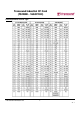
T Trraan nsscceen nd d IIn nd du ussttrriiaall C CF FC Caarrd d ((T TS S112288M M ~~ 1166G GC CF F110000II)) 29 Set Feature EFh Y – – – Y – Support 30 Set Multiple Mode C6h – Y – – Y – Support 31 Set Sleep Mode E6h or 99h – – – – Y – Support 32 Standby E2 or 96h – – – – Y – Support 33 Standby Immediate E0 or 94h – – – – Y – Support 34 Translate Sector 87h – Y Y Y Y Y Support 35 Wear Level F5h – – – – Y – Support 36 Write Buffer E8h –
T Trraan nsscceen nd d IIn nd du ussttrriiaall C CF FC Caarrd d ((T TS S112288M M ~~ 1166G GC CF F110000II)) Check Power Mode - 98h or E5h If the CompactFlash Storage Card is in, going to, or recovering from the sleep mode, the CompactFlash Storage Card sets BSY, sets the Sector Count Register to 00h, clears BSY and generates an interrupt. If the CompactFlash Storage Card is in Idle mode, the CompactFlash Storage Card sets BSY, sets the Sector Count Register to FFh, clears BSY and generates an interrupt.
T Trraan nsscceen nd d IIn nd du ussttrriiaall C CF FC Caarrd d ((T TS S112288M M ~~ 1166G GC CF F110000II)) Erase Sector(s) - C0h This command is used to pre-erase and condition data sectors in advance of a Write without Erase or Write Multiple without Erase command. There is no data transfer associated with this command but a Write Fault error status can occur. Flush Cache – E7h This command causes the card to complete writing data from its cache.
T Trraan nsscceen nd d IIn nd du ussttrriiaall C CF FC Caarrd d ((T TS S112288M M ~~ 1166G GC CF F110000II)) Identify Device – Ech The Identify Device command enables the host to receive parameter information from the CompactFlash Storage Card. This command has the same protocol as the Read Sector(s) command. The parameter words in the buffer have the arrangement and meanings defined in Table as below. All reserved bits or words are zero.
T Trraan nsscceen nd d IIn nd du ussttrriiaall C CF FC Caarrd d ((T TS S112288M M ~~ 1166G GC CF F110000II)) Word Address Default Value Total Bytes 51 0X00h 2 PIO data transfer cycle timing mode 52 0000h 2 Obsolete 53 000Xh 2 Field Validity 54 XXXXh 2 Current numbers of cylinders 55 XXXXh 2 Current numbers of heads 56 XXXXh 2 Current sectors per track 57-58 XXXXh 4 Current capacity in sectors (LBAs)(Word 57 = LSW, Word 58 = MSW) 59 01XXh 2 Multiple sector setting 60-61 XX
T Trraan nsscceen nd d IIn nd du ussttrriiaall C CF FC Caarrd d ((T TS S112288M M ~~ 1166G GC CF F110000II)) Word 0: General Configuration This field indicates the general characteristics of the device. When Word 0 of the Identify drive information is 848Ah then the device is a CompactFlash Storage Card and complies with the CFA specification and CFA command set. It is recommended that PCMCIA modes of operation report only the 848Ah value as they are always intended as removable devices.
T Trraan nsscceen nd d IIn nd du ussttrriiaall C CF FC Caarrd d ((T TS S112288M M ~~ 1166G GC CF F110000II)) Words 7-8: Number of Sectors per Card This field contains the number of sectors per CompactFlash Storage Card. This double word value is also the first invalid address in LBA translation mode. Words 10-19: Serial Number This field contains the serial number for this CompactFlash Storage Card and is right justified and padded with spaces (20h).
T Trraan nsscceen nd d IIn nd du ussttrriiaall C CF FC Caarrd d ((T TS S112288M M ~~ 1166G GC CF F110000II)) Multiple Sector Setting Bits 15-9 are reserved and shall be set to 0. Bit 8 shall be set to 1 indicating that the Multiple Sector Setting is valid. Bits 7-0 are the current setting for the number of sectors that shall be transferred per interrupt on Read/Write Multiple commands.
T Trraan nsscceen nd d IIn nd du ussttrriiaall C CF FC Caarrd d ((T TS S112288M M ~~ 1166G GC CF F110000II)) If this field is supported, bit 1 of word 53 shall be set to one. The value in word 66 shall not be less than the value in word 65. This field shall be supported by all CompactFlash Storage Cards supporting DMA modes 1 and above. If bit 1 of word 53 is set to one, but this field is not supported, the Card shall return a value of zero in this field.
T Trraan nsscceen nd d IIn nd du ussttrriiaall C CF FC Caarrd d ((T TS S112288M M ~~ 1166G GC CF F110000II)) If bit 3 of word 83 is set to one, the CompactFlash Storage Card supports the Advanced Power Management feature set. Bit 4 of word 83 shall be set to zero; the CompactFlash Storage Card does not support the Removable Media Status feature set. Words 85-87: Features/command sets enabled Words 85, 86, and 87 shall indicate features/command sets enabled.
T Trraan nsscceen nd d IIn nd du ussttrriiaall C CF FC Caarrd d ((T TS S112288M M ~~ 1166G GC CF F110000II)) Bit 2: 1 = Ultra DMA mode 2 and below are supported. Bits 0-1 Shall be set to 1. Bit 1: 1 = Ultra DMA mode 1 and below are supported. Bit 0 Shall be set to 1. Bit 0: 1 = Ultra DMA mode 0 is supported Word 89: Time required for Security erase unit completion Word 89 specifies the time required for the Security Erase Unit command to complete.
T Trraan nsscceen nd d IIn nd du ussttrriiaall C CF FC Caarrd d ((T TS S112288M M ~~ 1166G GC CF F110000II)) Bit 12: -XE If set to 1, indicates that Power Level 1 commands are disabled. If set to 0, indicates that Power Level 1 commands are enabled. Bit 0-11: Maximum current This field contains the CompactFlash Storage Card’s maximum current in mA.
T Trraan nsscceen nd d IIn nd du ussttrriiaall C CF FC Caarrd d ((T TS S112288M M ~~ 1166G GC CF F110000II)) 3-7 Reserved Bits 15-12 are reserved. Word 164: CF Advanced PCMCIA I/O and Memory Timing Modes Capabilities and Settings This word describes the capabilities and current settings for CFA defined advanced timing modes using the Memory and PCMCIA I/O interface.
T Trraan nsscceen nd d IIn nd du ussttrriiaall C CF FC Caarrd d ((T TS S112288M M ~~ 1166G GC CF F110000II)) Idle Immediate - 95h or E1h This command causes the CompactFlash Storage Card to set BSY, enter the Idle mode, clear BSY and generate an interrupt. Initialize Drive Parameters - 91h This command enables the host to set the number of sectors per track and the number of heads per cylinder. Only the Sector Count and the Card/Drive/Head registers are used by this command.
T Trraan nsscceen nd d IIn nd du ussttrriiaall C CF FC Caarrd d ((T TS S112288M M ~~ 1166G GC CF F110000II)) Read Buffer - E4h The Read Buffer command enables the host to read the current contents of the CompactFlash Storage Card’s sector buffer. This command has the same protocol as the Read Sector(s) command. Read DMA – C8h Read Long Sector - 22h or 23h Transcend Information Inc. 69 V1.
T Trraan nsscceen nd d IIn nd du ussttrriiaall C CF FC Caarrd d ((T TS S112288M M ~~ 1166G GC CF F110000II)) Read Multiple - C4h Read Sector(s) - 20h or 21h Read Verify Sector(s) - 40h or 41h Recalibrate - 1Xh Request Sense - 03h Transcend Information Inc. 70 V1.
T Trraan nsscceen nd d IIn nd du ussttrriiaall C CF FC Caarrd d ((T TS S112288M M ~~ 1166G GC CF F110000II)) The extended error code is returned to the host in the Error Register. Seek - 7Xh Set Features – EFh Transcend Information Inc. 71 V1.
T Trraan nsscceen nd d IIn nd du ussttrriiaall C CF FC Caarrd d ((T TS S112288M M ~~ 1166G GC CF F110000II)) Feature Supported Features 01h and 81h are used to enable and clear 8 bit data transfer modes in True IDE Mode. If the 01h feature command is issued all data transfers shall occur on the low order D[7:0] data bus and the -IOIS16 signal shall not be asserted for data register accesses. The host shall not enable this feature for DMA transfers.
T Trraan nsscceen nd d IIn nd du ussttrriiaall C CF FC Caarrd d ((T TS S112288M M ~~ 1166G GC CF F110000II)) Feature 03h allows the host to select the PIO or Multiword DMA transfer mode by specifying a value in the Sector Count register. The upper 5 bits define the type of transfer and the low order 3 bits encode the mode value. One PIO mode shall be selected at all times. For Cards which support DMA, one Multiword DMA mode shall be selected at all times.
T Trraan nsscceen nd d IIn nd du ussttrriiaall C CF FC Caarrd d ((T TS S112288M M ~~ 1166G GC CF F110000II)) Standby Immediate - 94h or E0h Translate Sector - 87h Translate Sector Information Transcend Information Inc. 74 V1.
T Trraan nsscceen nd d IIn nd du ussttrriiaall C CF FC Caarrd d ((T TS S112288M M ~~ 1166G GC CF F110000II)) Wear Level - F5h Write Buffer - E8h Write DMA – CAh Transcend Information Inc. 75 V1.
T Trraan nsscceen nd d IIn nd du ussttrriiaall C CF FC Caarrd d ((T TS S112288M M ~~ 1166G GC CF F110000II)) Write Long Sector - 32h or 33h Write Multiple Command - C5h Write Multiple without Erase – CDh Transcend Information Inc. 76 V1.
T Trraan nsscceen nd d IIn nd du ussttrriiaall C CF FC Caarrd d ((T TS S112288M M ~~ 1166G GC CF F110000II)) Write Sector(s) - 30h or 31h Write Sector(s) without Erase - 38h Write Verify - 3Ch Transcend Information Inc. 77 V1.
T Trraan nsscceen nd d IIn nd du ussttrriiaall C CF FC Caarrd d ((T TS S112288M M ~~ 1166G GC CF F110000II)) Error Posting Transcend Information Inc. 78 V1.
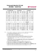
T Trraan nsscceen nd d IIn nd du ussttrriiaall C CF FC Caarrd d ((T TS S112288M M ~~ 1166G GC CF F110000II)) Error and Status Register summarizes the valid status and error value for all the CF-ATA Command set. SMART Command Set SMART Command Set SMART Feature Register Values D0h Read Data D4h Execute OFF-LINE Immediate D1h Read Attribute Threshold D8h Enable SMART Operations D2h Enable/Disable Autosave D9h Disable SMART Operations D3h Save Attribute Values DAh Return Status 1.
T Trraan nsscceen nd d IIn nd du ussttrriiaall C CF FC Caarrd d ((T TS S112288M M ~~ 1166G GC CF F110000II)) SMART Data Structure BYTE F/V Decription 0-1 X Revision code 2-361 X Vendor specific 362 V Off line data collection status 363 X Self-test execution status byte 364-365 V Total time in seconds to complete off-line data collection activity 366 X Vendor specific 367 F Off-line data collection capability 368-369 F 370 F SMART capability Error logging capability 7-1 Reserved